
Samsung 4 nm Lines Reach Full Utilization as HBM4 Takes Up to 60% of Capacity
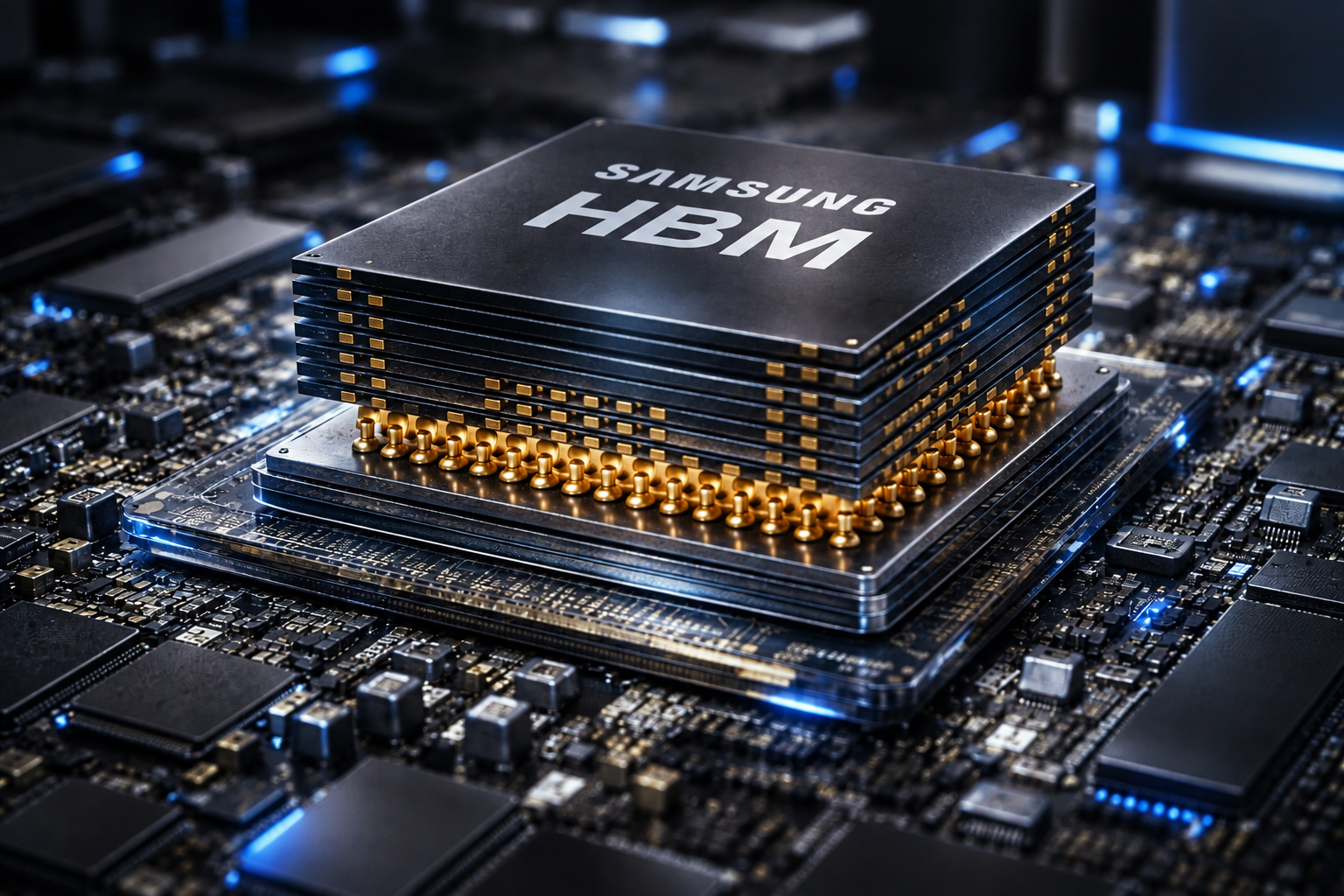
Samsung Electronics is pushing its HBM4 production ramp aggressively, with its 4 nm foundry lines reportedly operating at full utilization while HBM4 base dies now consume between 50% and 60% of available 4 nm capacity. The increase reflects rapidly growing demand for next generation AI accelerators and marks another significant improvement for a foundry business that only recently faced persistent questions around utilization, yields, and profitability. According to industry reporting from South Korea, Samsung began substantially increasing wafer input for HBM4 base die production around the middle of 2026 as it prepared for much larger shipments during the second half of the year.
Samsung currently produces advanced processes ranging from approximately 4 nm to 7 nm across its Pyeongtaek foundry facilities, with available 4 nm capacity estimated at roughly 30,000 wafers per month. Industry estimates indicate more than half of that capacity is now being allocated specifically to HBM4 base dies, suggesting approximately 15,000 or more 4 nm wafers per month could be entering production for HBM4 alone. An industry source familiar with the situation says HBM4 base dies are currently responsible for roughly 50% to 60% of Samsung's 4 nm production while the lines remain under full production conditions. These figures remain industry estimates rather than official capacity disclosures from Samsung.
The base die has become increasingly important with HBM4 because it sits underneath the vertically stacked DRAM dies and manages communication between the memory stack and the processor or accelerator. Samsung manufactures its HBM4 base die using its SF4 4 nm foundry process while pairing it with sixth generation 10 nm class 1c DRAM. The company began commercial HBM4 production and shipments in February 2026, and its improving manufacturing efficiency has already produced another major milestone, with Samsung HBM4 yields reportedly approaching 80%.
That combination of stronger yields and increasing capacity is becoming critical as NVIDIA, AMD, Broadcom, and other AI processor developers prepare larger deployments of platforms requiring HBM4. NVIDIA's Vera Rubin generation is particularly significant, with each Rubin GPU integrating 288 GB of HBM4 and delivering enormous memory bandwidth. At rack scale, NVIDIA Vera Rubin NVL72 can carry approximately 20.7 TB of HBM4, demonstrating how quickly individual AI deployments can consume advanced memory production capacity.
Samsung itself expects the HBM4 ramp to accelerate considerably. During its Q2 2026 earnings discussions, the company said HBM4 revenue during Q3 was expected to increase more than 3 times compared with Q2, while HBM4 is expected to represent more than 60% of Samsung's total HBM revenue during the second half of 2026. That 60% revenue figure is separate from the reported 50% to 60% share of 4 nm foundry capacity now being consumed by HBM4 base dies.
The production surge also strengthens the turnaround story surrounding Samsung Foundry. Earlier in 2026, Samsung's 4 nm demand was already pushing its foundry business toward significantly higher utilization, with HBM4 base dies becoming one of the primary drivers alongside external AI chip orders. More recent reporting indicates the Pyeongtaek 4 nm operation has approached 100% utilization, while improved process stability has helped Samsung secure additional advanced semiconductor production.
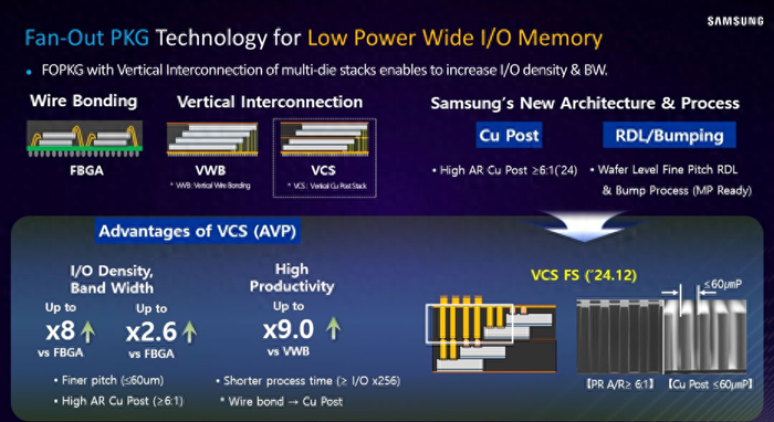
The situation also illustrates how HBM is becoming more tightly connected with the foundry industry. Previous HBM generations were primarily viewed as specialized memory products, but HBM4 introduces increasingly sophisticated logic into the base die, requiring advanced manufacturing processes traditionally associated with processors and accelerators. Samsung already plans to take this further, with 2 nm base die technology expected for future HBM generations.
HBM4 is doing more than strengthening Samsung's memory business. It is becoming a major customer of Samsung Foundry itself. Allocating as much as 60% of available 4 nm capacity to HBM4 base dies shows how AI memory is increasingly consuming advanced logic manufacturing resources alongside GPUs, CPUs, and custom accelerators.
That creates an unusual strategic advantage for Samsung because it controls DRAM manufacturing, logic foundry production, and advanced packaging within the same semiconductor organization. If HBM4 demand remains strong and yields continue improving, Samsung could benefit from the AI memory boom across several stages of the manufacturing chain instead of simply selling DRAM stacks.
Could HBM4 become the product that finally drives a sustained Samsung Foundry recovery, or will external foundry customers still be necessary for Samsung to challenge TSMC more seriously?
