
Samsung Reportedly Prepares 2 nm HBM Base Die Production as AI Memory Roadmap Accelerates

Samsung Electronics is reportedly preparing additional foundry capacity for 2 nm HBM base dies, potentially giving the company dedicated manufacturing infrastructure as HBM moves beyond the current 4 nm generation. According to ZDNet Korea, Samsung is considering converting the second line of its NRD K semiconductor research complex in Giheung into foundry production capacity focused primarily on advanced HBM logic base dies.
The NRD K 2 facility is currently under construction and is reportedly targeting an opening during 2H 2028. Samsung plans to invest approximately 20 trillion won across the wider NRD K complex through 2030, with the second line potentially operating as a send fab that receives wafers from other production facilities for selected advanced processing stages. Industry sources cited by ZDNet Korea claim one of its primary targets could be 2 nm HBM base dies intended for major AI customers including NVIDIA, although Samsung has not officially confirmed that customer allocation.
The transition to 2 nm is already part of Samsung's HBM technology roadmap. Samsung Foundry executive Ja Heum Koo previously confirmed that HBM5 will adopt a 2 nm GAA base die, replacing the 4 nm logic technology used by HBM4 and HBM4E. Samsung expects HBM5 operating speeds to improve by more than 50% compared with HBM4E, requiring higher logic density, improved power efficiency, and more advanced TSV integration.
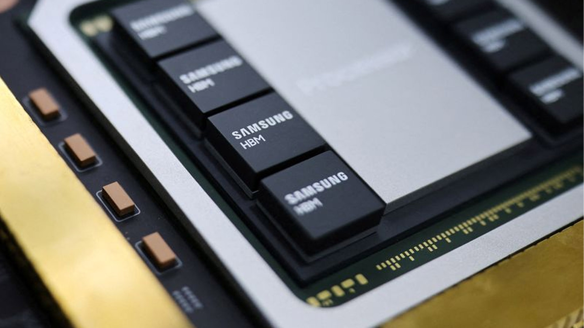
Samsung currently manufactures its commercial HBM4 using 1c DRAM and a 4 nm logic base die. The memory delivers a consistent 11.7 Gbps per pin, can scale to 13 Gbps, and provides as much as 3.3 TB/s of bandwidth per stack. Samsung entered mass production in February 2026 and has since reportedly pushed HBM4 manufacturing yield toward 80%, strengthening its ability to increase AI memory shipments without requiring equivalent growth in wafer capacity.
The company is keeping the same 4 nm base die for HBM4E, which reaches a stable 14 Gbps and can scale to 16 Gbps, delivering up to 3.6 TB/s of bandwidth from a 48 GB 12 layer stack. Samsung began shipping HBM4E samples in May and plans to begin mass production according to customer qualification schedules.
Samsung's ability to manufacture DRAM, logic base dies, and advanced packaging internally could become increasingly valuable as HBM becomes more customized for individual AI processors. Competitors are moving aggressively as well, with SK hynix already sampling 48 GB HBM4E at 16 Gbps, making manufacturing scale, power efficiency, thermal control, and customer qualification increasingly important alongside raw bandwidth.
The move from 4 nm to 2 nm shows how the HBM base die is evolving from a relatively simple interface component into increasingly advanced logic silicon. Samsung has a unique advantage because its Memory and Foundry businesses can develop both sides internally. If NRD K 2 ultimately becomes dedicated capacity for 2 nm HBM logic, Samsung could control more of the AI memory manufacturing chain while reducing its dependence on external foundries. The important distinction is that the 2 nm HBM5 roadmap is confirmed, while the specific NRD K 2 production plan and reported NVIDIA allocation remain subject to change before the facility opens in 2028.
Could Samsung's ability to combine its own DRAM, 2 nm foundry technology, and advanced packaging become its biggest advantage against SK hynix and Micron in future HBM generations?
