
NVIDIA NVHBM Could Reshape HBM Economics as Base Die Costs Rise
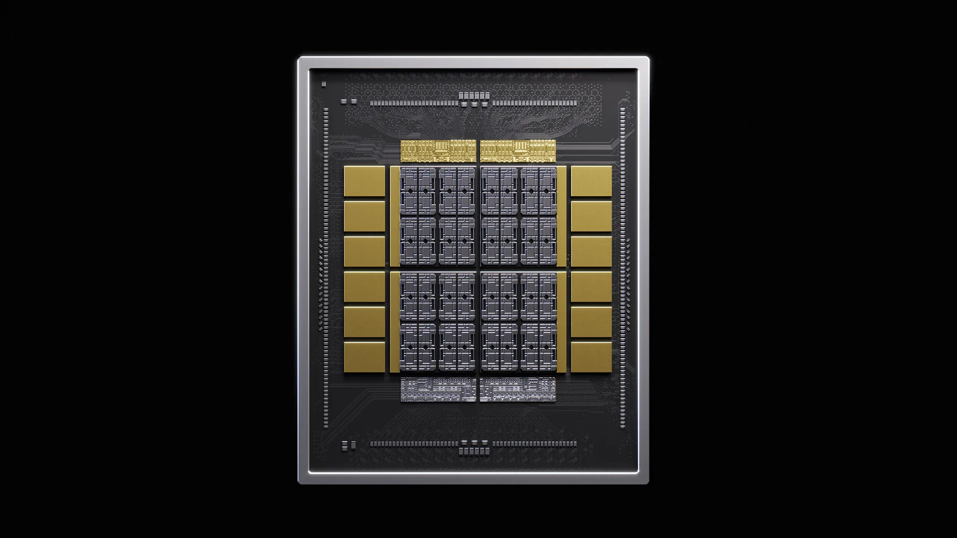
NVIDIA's recently announced NVHBM architecture may have implications reaching far beyond its promised improvements in memory bandwidth and power efficiency. As the logic base die becomes an increasingly expensive and sophisticated component of next generation HBM, NVIDIA's decision to design its own base die and integrate its proprietary memory controller directly into the stack could shift a larger portion of the technology, intellectual property and economic value surrounding AI memory toward NVIDIA itself.
The discussion intensified after industry reports claimed that the logic base die used by SK hynix for HBM4, manufactured using a TSMC 12 nm class process, could cost approximately 3 to 4 times as much as a single DRAM core die manufactured using SK hynix's own 1b process. TrendForce reported the estimate while covering claims that SK hynix is evaluating Intel Foundry as an additional supplier for future HBM4E base dies. SK hynix subsequently said portions of the original report were inaccurate without identifying the specific claims it disputed.
The distinction between one DRAM die and an entire HBM stack is important. A modern HBM product can contain 12 or more vertically stacked DRAM dies above a single logic base die, meaning a base die costing 3 to 4 times more than one core die does not automatically represent the majority of the total manufacturing value of the complete stack. Packaging, testing, stacking and yield also contribute substantially to HBM cost. Even so, the base die is rapidly becoming one of the most technologically valuable individual components as more logic moves into the bottom layer.
HBM4 marks an important transition in this direction. Earlier HBM generations could use relatively straightforward base dies manufactured using memory oriented processes, but the growing bandwidth, interface and control requirements of HBM4 have pushed manufacturers toward more advanced logic processes. SK hynix moved HBM4 base die manufacturing to TSMC, while Samsung produces its current HBM4 with a 4 nm logic base die. Samsung is already preparing even more advanced logic technology, with 2 nm base dies planned for future HBM5.
NVIDIA's NVHBM takes that evolution considerably further. Instead of leaving the complete HBM interface architecture to the memory manufacturer, NVIDIA has designed a custom base die containing its own memory controller and PHY. Traditional HBM places the memory controller on the GPU or XPU compute die. With NVHBM, NVIDIA moves that controller directly underneath the DRAM stack. NVIDIA says this reduces the PHY and supporting area by as much as 67% compared with standard HBM4E and significantly simplifies connections between the memory and accelerator.
The architectural benefits are substantial. NVIDIA claims NVHBM can provide up to 30% more memory bandwidth, reduce HBM power consumption by as much as 15%, and free up to 25% more area on the XPU compute die compared with conventional HBM4E. Its broader package analysis suggests the redesigned interface can make as much as 30% more main die silicon available for compute and other functionality. NVIDIA estimates that these improvements can combine with NVLink Fusion to deliver as much as a 30% end to end performance improvement per XPU.
These performance gains were the focus when NVIDIA originally unveiled NVHBM, but the economic implications are becoming equally interesting. If the logic base die continues moving toward more advanced and expensive semiconductor processes, ownership of the design becomes increasingly valuable. NVIDIA would control the memory controller, PHY and custom logic while memory manufacturers provide compatible DRAM dies, manufacturing expertise, stacking and qualification.
NVIDIA is also deliberately designing NVHBM around multiple suppliers. The company says it will establish a standardized NVHBM implementation that can be validated and offered by leading memory manufacturers. This could allow companies developing custom accelerators through NVLink Fusion to qualify the same NVIDIA controlled memory architecture across more than one HBM supplier instead of creating substantially different implementations for Samsung, SK hynix or Micron. Amazon's Annapurna Labs will become the first announced company to collaborate with NVIDIA on NVHBM.
That strategy potentially gives NVIDIA additional negotiating leverage. Samsung, SK hynix and Micron currently compete heavily on complete HBM products, including bandwidth, capacity, power consumption, stacking technology and manufacturing yield. Under NVHBM, more of the differentiated logic and interface technology would originate from NVIDIA, potentially making the underlying DRAM portion easier to source from multiple qualified manufacturers.
It would nevertheless be premature to describe the major memory manufacturers as commodity suppliers. Manufacturing HBM remains exceptionally difficult, and memory die quality, stacking technology, thermals, yields and production capacity remain fundamental competitive advantages. Samsung, SK hynix and Micron are also developing increasingly customized HBM products of their own. SK hynix has already sampled 48 GB HBM4E operating at up to 16 Gbps, while Samsung continues investing in increasingly advanced logic base dies and packaging technologies.
The reported HBM4 base die cost nevertheless illustrates why the architecture is becoming strategically important. Moving from relatively simple base silicon toward advanced logic processes increases the portion of HBM cost associated with technology other than the DRAM cells themselves. NVIDIA inserting its own architecture into that layer gives the company influence over another critical component of the AI accelerator supply chain.
NVHBM may ultimately be more important as a business strategy than the initial 30% bandwidth improvement suggests.
The key detail is not that a base die reportedly costs 3 to 4 times as much as the entire HBM memory stack. It does not. The comparison is with a single DRAM core die, and modern HBM contains many of those dies. However, the base die is becoming far more complex, expensive and strategically important as memory interfaces evolve.
That creates an opportunity for NVIDIA. By owning the memory controller, PHY and custom base die architecture, NVIDIA gains control over another layer of technology that was previously largely contained within the accelerator and memory supplier relationship. At the same time, supporting multiple memory providers could strengthen its ability to negotiate supply and reduce dependence on any single HBM manufacturer.
Samsung, SK hynix and Micron are unlikely to become simple commodity vendors anytime soon, especially while AI demand keeps advanced HBM capacity scarce. But NVHBM does shift the balance. NVIDIA is no longer simply buying high bandwidth memory. It is beginning to define more of what that memory actually is.
Could NVIDIA's control of the NVHBM base die eventually reduce the pricing power of Samsung, SK hynix and Micron, or will advanced HBM manufacturing remain too specialized for memory suppliers to lose their leverage?
