
NVIDIA Unveils NVHBM With 30% More Bandwidth and Lower Power Than HBM4E
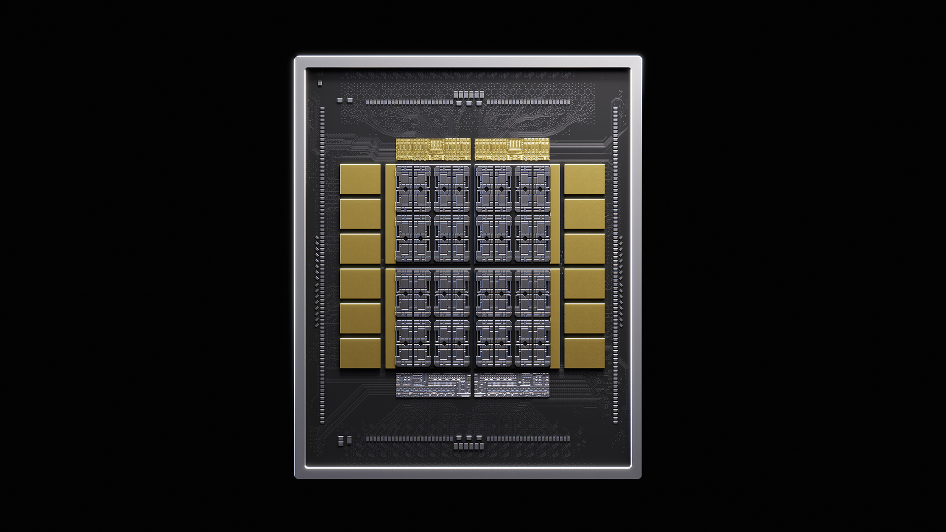
NVIDIA has introduced NVHBM, a custom high bandwidth memory architecture designed for future AI accelerators as memory bandwidth, power consumption and silicon area become increasingly important limitations for large scale artificial intelligence infrastructure. According to NVIDIA's official NVHBM technical overview, NVHBM can provide up to 30% more memory bandwidth per stack and consume up to 15% less HBM power compared with standard HBM4E.
The architectural change comes from moving the memory controller away from the main XPU compute die and integrating NVIDIA's custom controller directly into the HBM base die alongside a redesigned PHY. NVIDIA says this approach reduces PHY and supporting area by as much as 67% compared with the JEDEC HBM4E design while simplifying interposer routing. More efficient memory connections can free up to 25% additional compute die area for XPU functionality, while NVIDIA's broader layout analysis indicates as much as 30% more main die silicon can potentially become available for compute or other features.
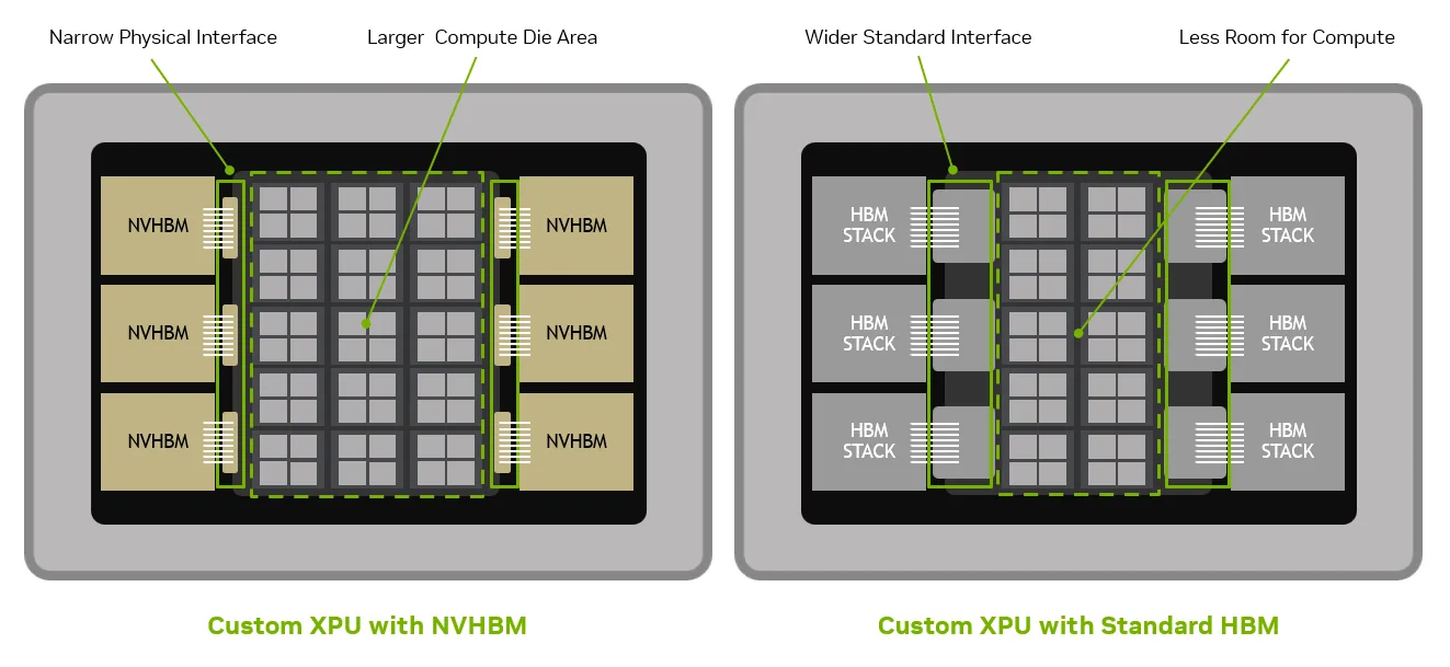
For AI accelerators, these improvements directly target the growing memory bottleneck created by large models, reasoning workloads, KV cache traffic and increasingly demanding inference operations. NVIDIA estimates that combining the additional memory bandwidth, compute area and reduced HBM power through NVHBM and NVLink Fusion can produce up to a 30% overall end to end performance improvement per XPU. At the scale of a 1 GW data center populated with 2,000W XPUs, NVIDIA estimates the memory power savings could create enough electrical headroom for as many as 15,000 additional XPUs.
| Feature | NVHBM Benefit |
|---|---|
| Bandwidth | Up to 30% more memory bandwidth compared with standard HBM4e |
| Area | More efficient interface connections allow up to 25% more compute die area for additional XPU capabilities |
| Power | Up to 15% lower HBM power usage compared with standard HBM4e, adding up to significant savings across thousands of XPUs |
The announcement arrives as the industry's AI memory bandwidth problem continues to intensify and memory suppliers push technologies such as 48 GB HBM4E running at up to 16 Gbps. NVIDIA also plans to establish NVHBM as a standardized implementation available through multiple memory suppliers, reducing the engineering and qualification work required for companies developing custom accelerators. Amazon's Annapurna Labs will be the first announced collaborator and plans to combine NVHBM with NVLink Fusion as its future Trainium architecture becomes increasingly integrated with NVIDIA's rack scale infrastructure, according to NVIDIA.
"NVHBM represents a new architectural approach to advancing high bandwidth memory performance and efficiency."
— Quote by: Nafea Bshara, Vice President of Annapurna Labs at Amazon.
NVIDIA has confirmed that NVHBM is intended for future GPUs and custom AI accelerators, positioning the technology as part of a broader strategy to improve memory efficiency and system level performance as next generation AI platforms continue scaling in compute density and power requirements.
NVHBM represents a significant shift because NVIDIA is no longer treating HBM simply as memory attached to an accelerator. Moving part of the memory architecture into the HBM stack creates another opportunity to improve compute density, bandwidth and power efficiency without relying exclusively on increasingly large GPU dies. With AI infrastructure already placing enormous pressure on HBM capacity, pricing and power consumption, tighter integration between memory suppliers and accelerator designers could become one of the defining architectural trends of the next generation of AI hardware.
Could custom memory architectures such as NVHBM become just as important as the GPU architecture itself for future AI performance?
