
Fujitsu MONAKA Stacks 2 nm CPU Cores Over 5 nm SRAM as MONAKA X Targets 1.4 nm in 2029
Fujitsu has provided its most detailed look yet at FUJITSU MONAKA, revealing how its upcoming 144 core Arm processor combines TSMC 2 nm compute silicon with 5 nm SRAM and I O dies through an advanced 3D chiplet architecture. Presented at Hot Chips 2026, MONAKA is scheduled for production shipments in 2027 and targets AI inference, cloud computing and high performance computing with a strong emphasis on power efficiency. Fujitsu is also already looking further ahead with FUJITSU MONAKA X, a 1.4 nm successor planned for 2029 that will support Arm SME2 and tightly connect with NVIDIA GPUs through NVLink Fusion.
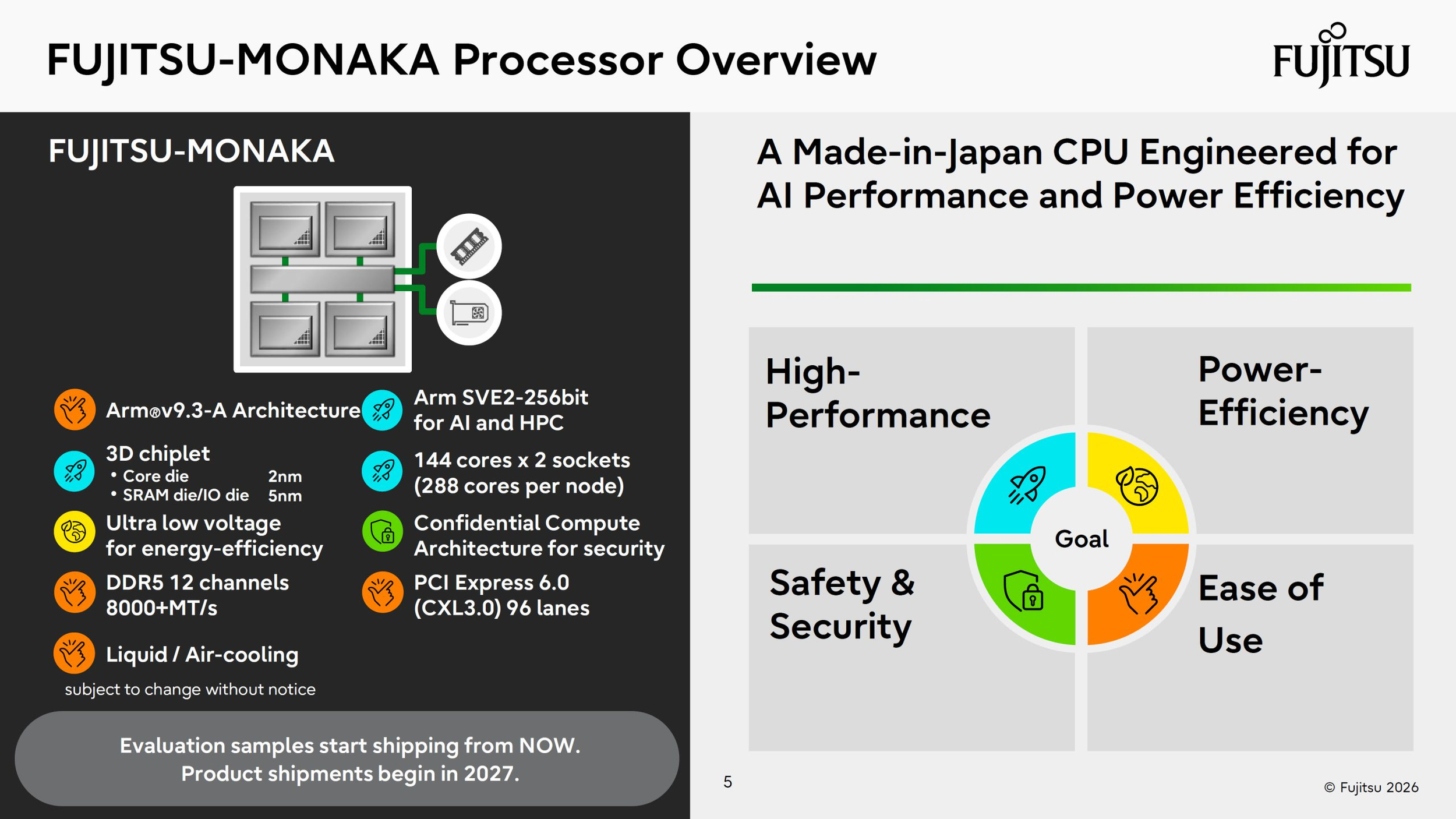
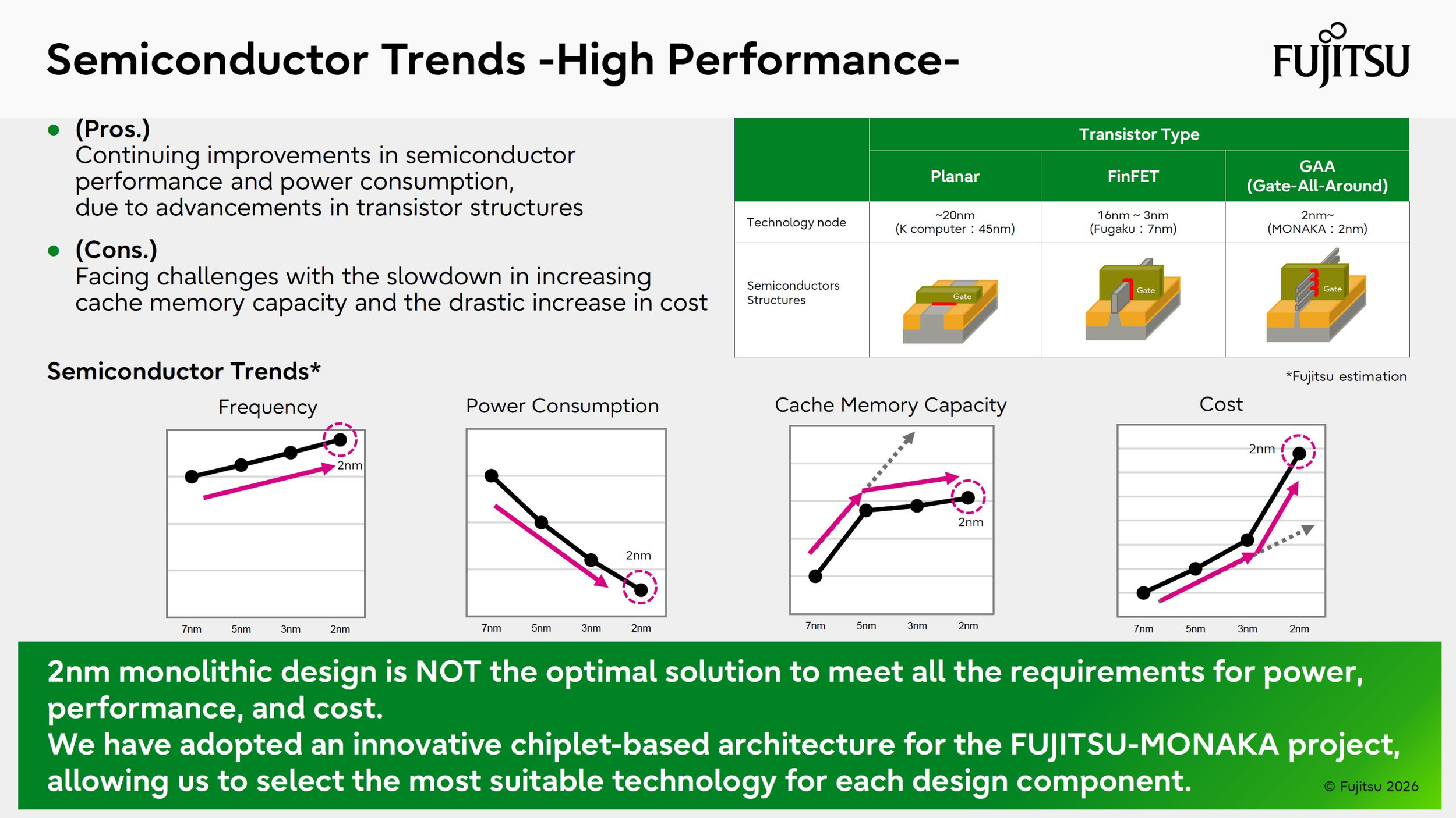
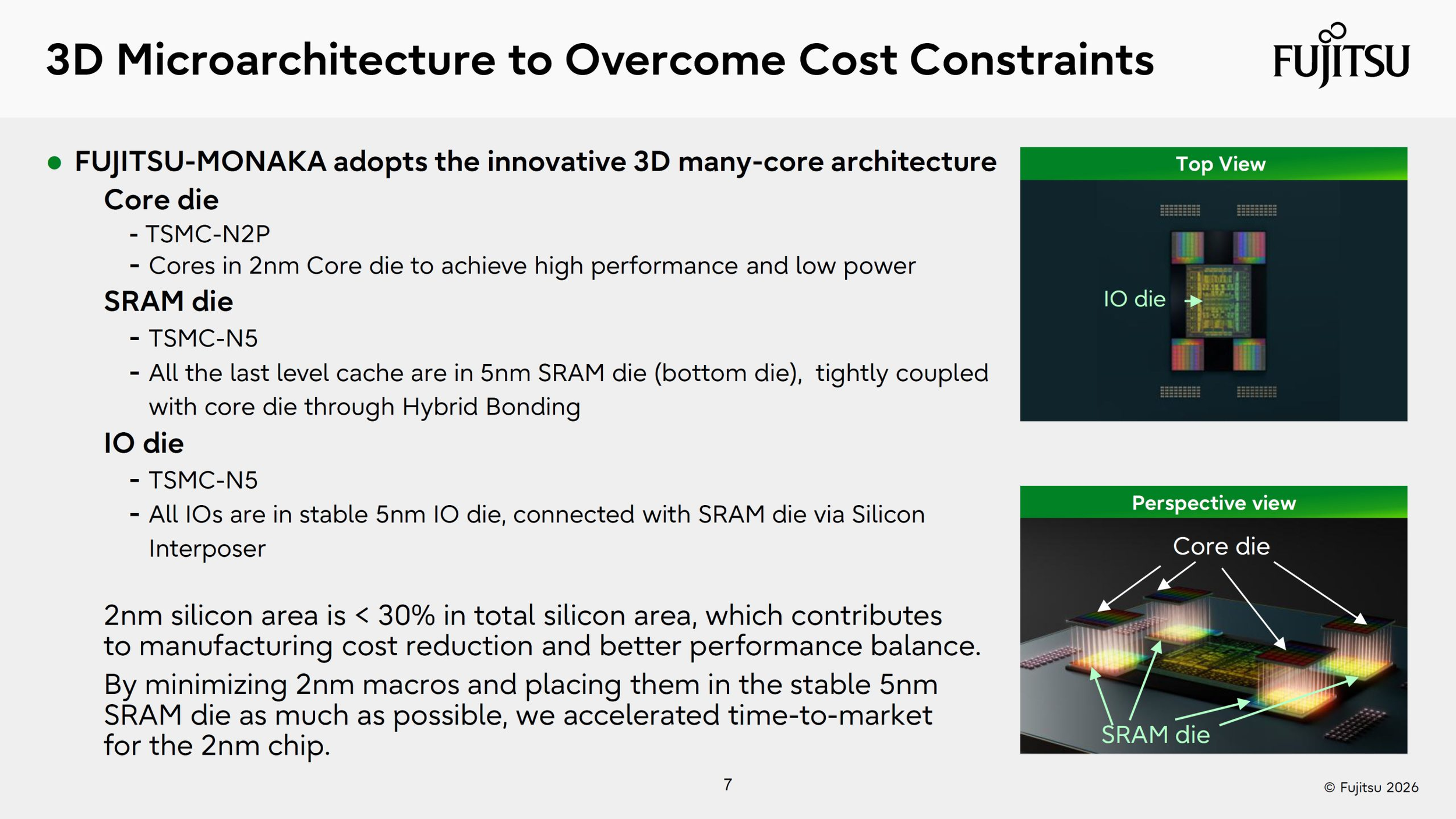
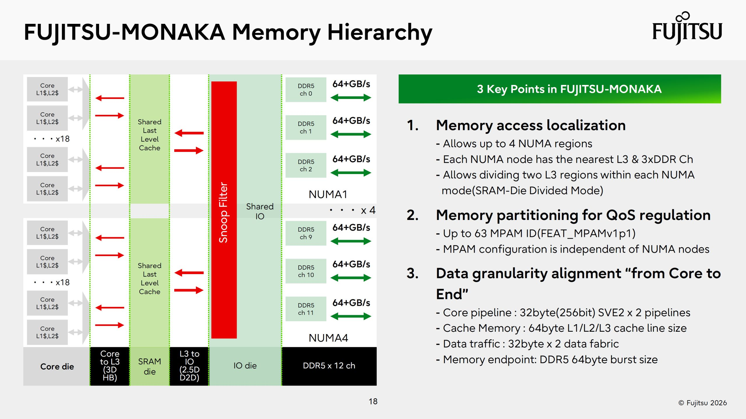
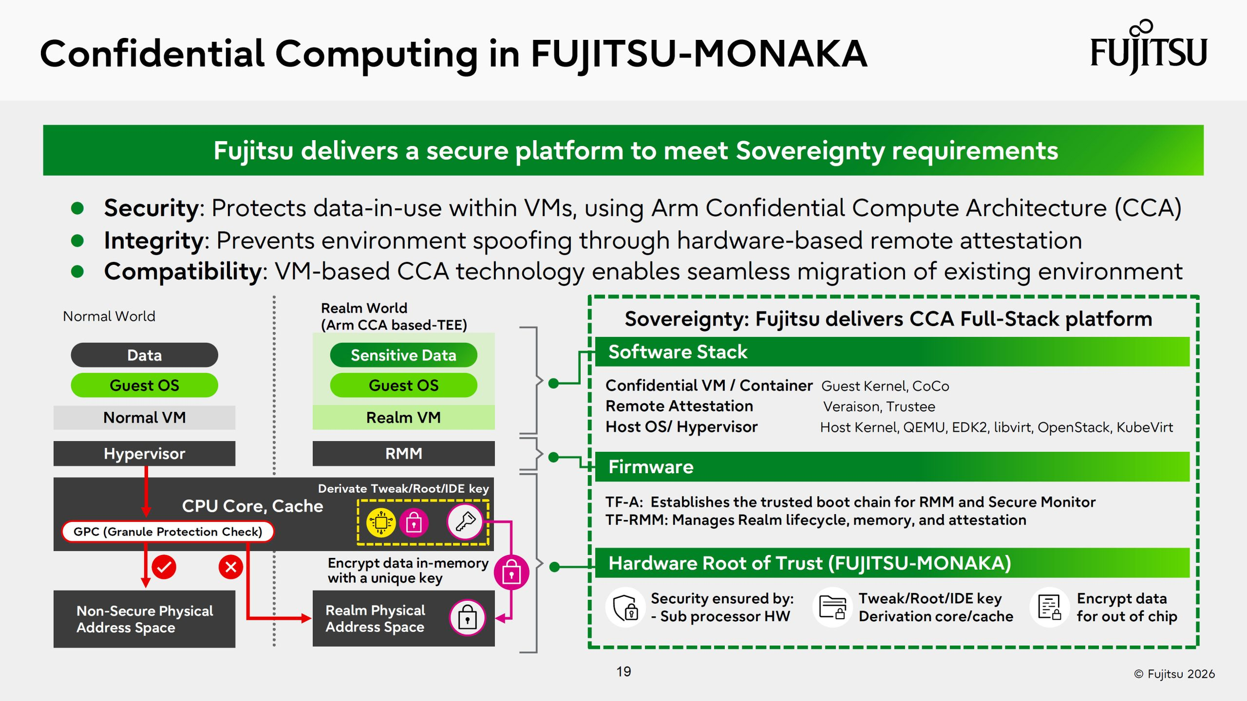
The most interesting part of MONAKA is how Fujitsu distributes its silicon. Instead of building the complete processor on an expensive leading edge process, the company uses TSMC N2P for the CPU core dies while moving the entire last level cache onto separate 5 nm SRAM dies underneath them. The SRAM and I O silicon use TSMC N5, with the core and cache dies connected through face to face hybrid bonding and the I O die communicating through a silicon interposer. According to Fujitsu, less than 30% of the processor's total silicon area requires the advanced 2 nm process, allowing the company to reserve expensive leading edge manufacturing for the circuits that benefit most from higher transistor density and efficiency.
Positioning the SRAM directly below the CPU cores also shortens communication distances between compute and cache. Fujitsu places the hotter compute die on top of the stack to provide a shorter thermal path toward the cooling system, while integrated voltage regulation enables individual core voltage and frequency control. The result is an architecture designed simultaneously around latency, power efficiency, manufacturing cost and thermal management rather than simply maximizing the amount of 2 nm silicon inside the package.
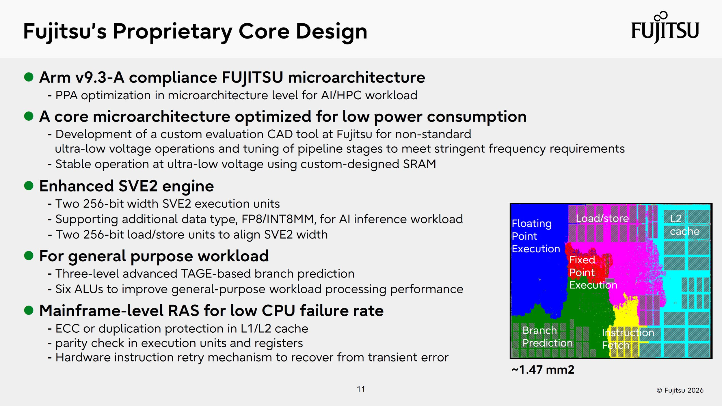
MONAKA contains 144 custom Arm v9.3 A CPU cores and supports 2 socket systems with as many as 288 cores per node. Each core incorporates 2 256 bit SVE2 execution units and 2 256 bit load and store units, while additional data types including FP8 and INT8 matrix operations target AI inference. Fujitsu is also incorporating extensive reliability features including ECC protection across cache, parity protection for execution hardware and registers, and a hardware instruction retry mechanism designed to recover from transient errors.
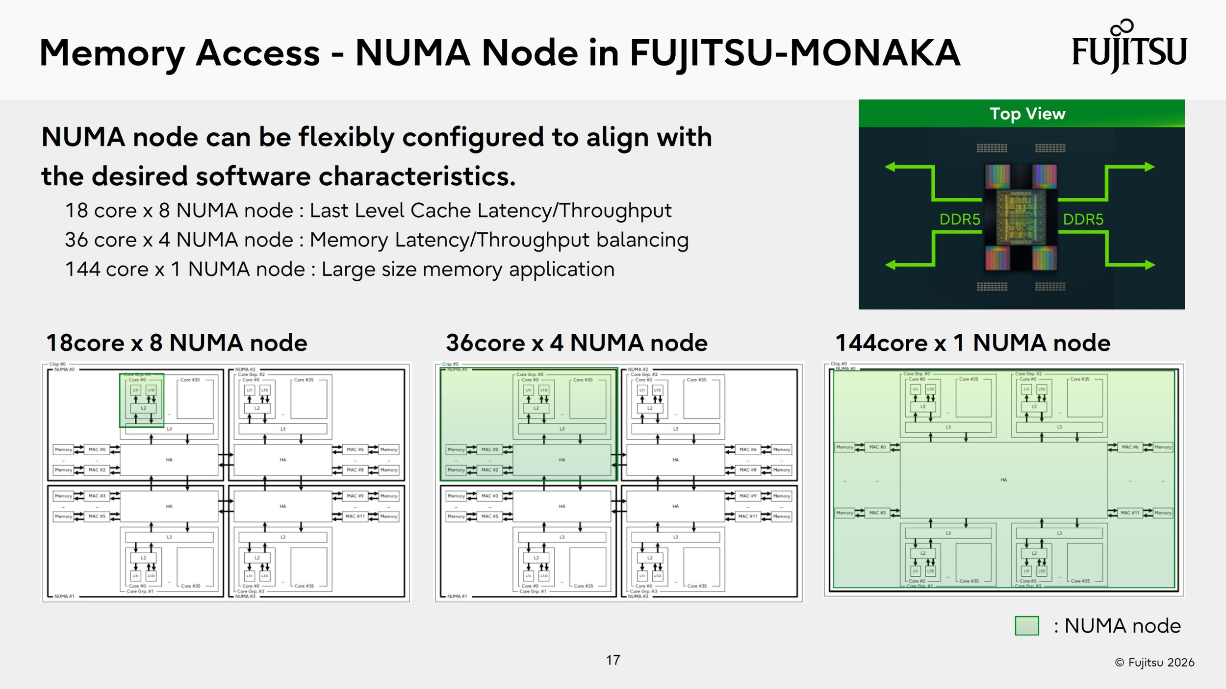
Memory and connectivity are equally aggressive. MONAKA supports 12 channels of DDR5 operating beyond 8000 MT/s and provides 96 lanes of PCI Express 6.0 with CXL 3.0 support. Fujitsu can also configure the 144 cores into different NUMA arrangements, including 8 groups of 18 cores, 4 groups of 36 cores or a single 144 core NUMA domain depending on whether workloads prioritize cache latency, memory throughput or access to larger memory spaces.
Fujitsu is preparing 2 performance configurations. The high performance version uses all 144 cores at a 2.9 GHz base frequency with a 500 W power target and liquid cooling, while the efficiency focused version operates at 2.1 GHz and 350 W with air cooling. Fujitsu estimates approximately 6,013 GFLOPS of DGEMM performance and 96.2 TOPS of INT8 performance from the 500 W model at base frequency, while the 350 W configuration targets 4,355 GFLOPS and 69.7 TOPS. Evaluation systems are already available, with commercial production planned for 2027.
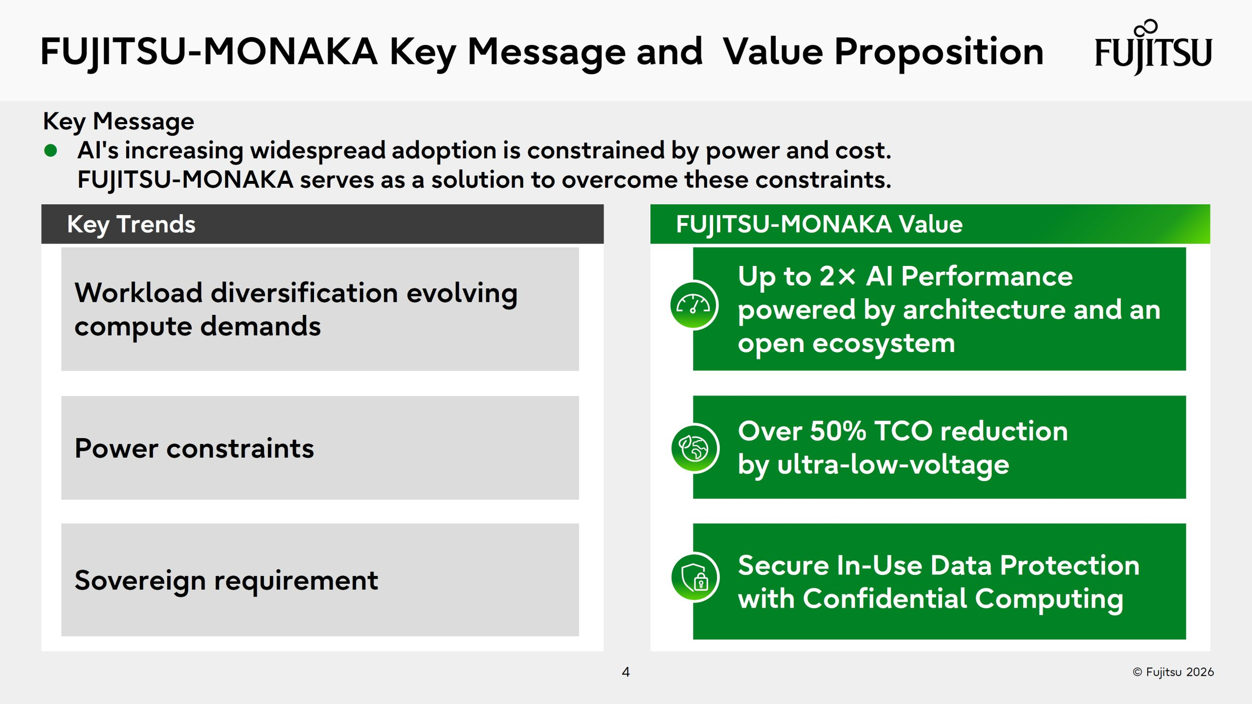
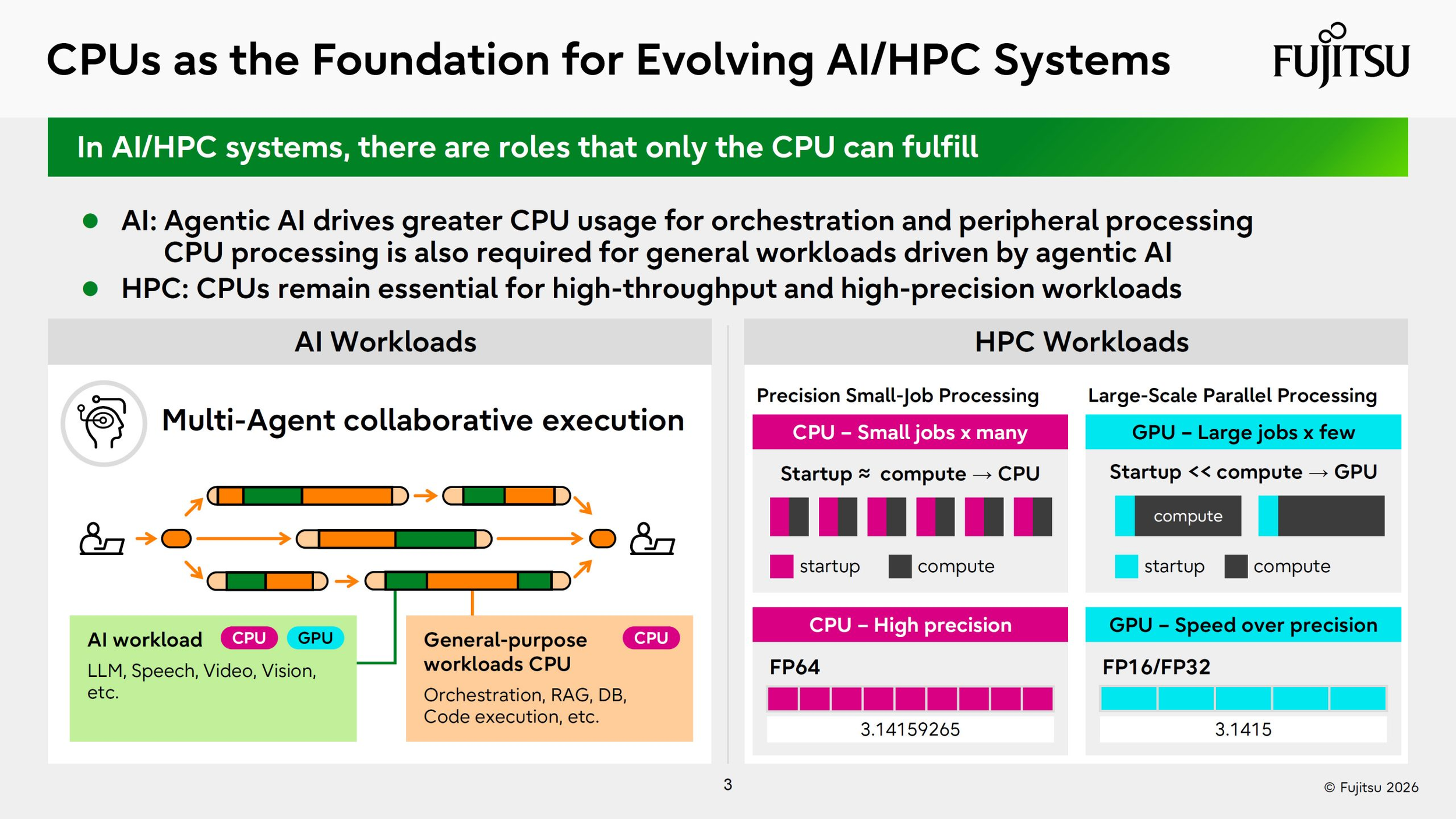
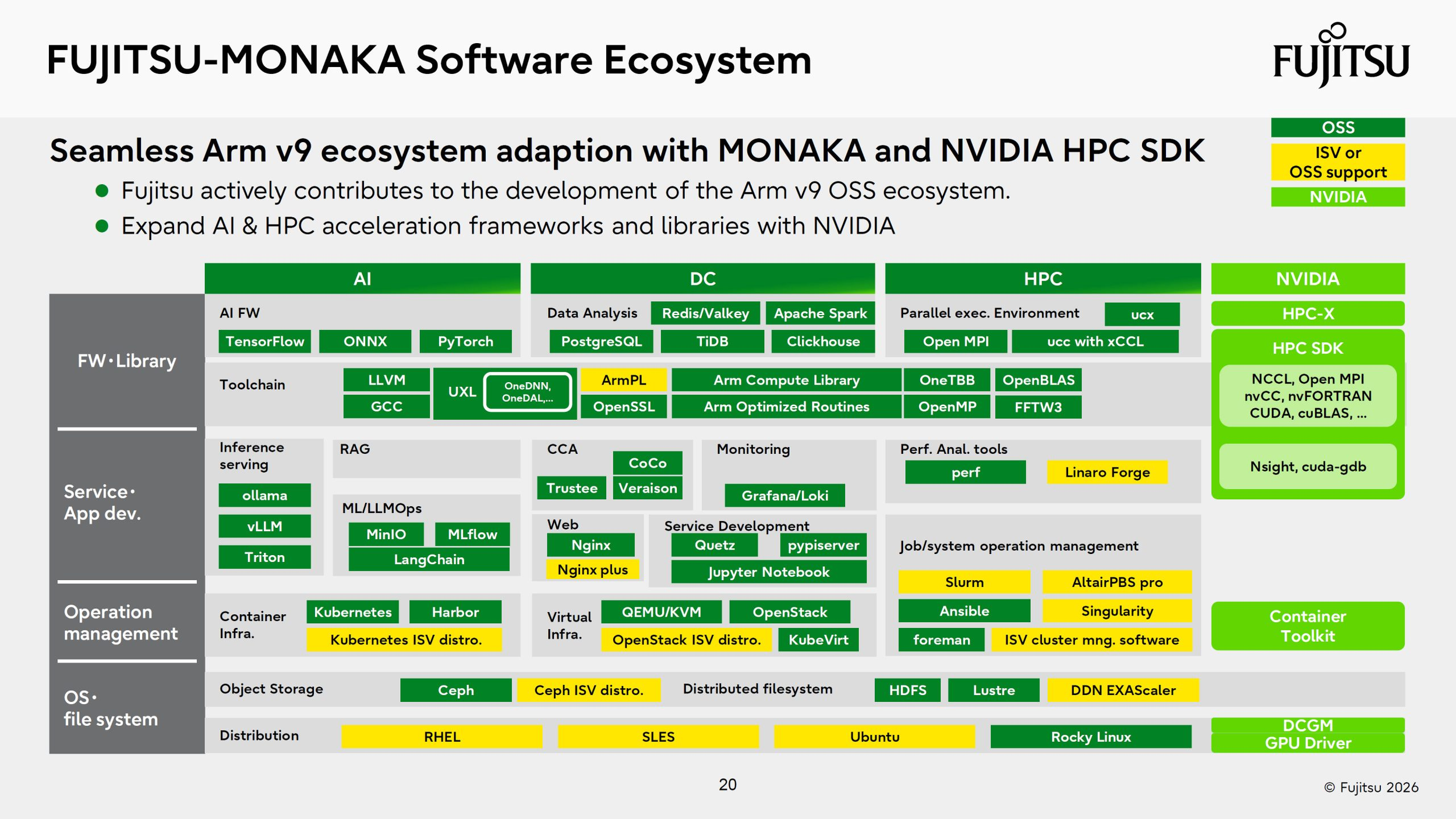
The architecture also reflects Fujitsu's belief that CPUs will remain increasingly important as AI infrastructure shifts toward agentic workloads. GPUs can handle enormous amounts of parallel computation, but CPUs remain responsible for orchestration, irregular data movement, databases, networking, system management and many of the latency sensitive operations surrounding AI accelerators. Fujitsu is targeting up to 2x the AI performance per watt of competing 2027 CPUs while aiming to reduce total cost of ownership through ultra low voltage operation. These remain Fujitsu projections and will require independent testing once production hardware becomes available.
The longer term roadmap becomes considerably more ambitious with MONAKA X. Fujitsu Research says the 2029 processor will move from 144 cores to more than 200 cores while transitioning the core die from 2 nm to a 1.4 nm class process. It will retain the company's 3D many core strategy while adding Arm SME2 matrix acceleration specifically for AI workloads.
MONAKA X is also being designed around much tighter CPU and GPU cooperation. Fujitsu will use NVIDIA NVLink Fusion to provide high bandwidth, low latency and memory coherent communication between MONAKA X CPUs and NVIDIA GPUs. Instead of repeatedly copying data between separate CPU and GPU memory spaces, Fujitsu wants both processors to operate with a much more unified view of memory, allowing the CPU to handle complex control flow and latency sensitive work while NVIDIA GPUs execute massively parallel computation.
This architecture will become central to Japan's next flagship supercomputer. RIKEN's FugakuNEXT technical plan confirms MONAKA X as its CPU platform, with the system combining SVE2, SME2, advanced 3D chiplets and tightly coupled NVIDIA GPU acceleration. FugakuNEXT is being designed around the convergence of traditional HPC and modern AI rather than repeating the CPU only architecture of the current Fugaku system.
The strategy also places Fujitsu inside a wider industry movement toward heterogeneous AI infrastructure. NVIDIA has increasingly opened its rack scale ecosystem to external processors through NVLink Fusion, while companies across the industry are building systems where CPUs, GPUs and specialized accelerators operate as parts of a unified compute platform. NVIDIA's growing relationship with Japan has already extended across AI infrastructure, robotics and semiconductor partnerships, as seen during Jensen Huang's recent meetings with Fujitsu and other Japanese technology leaders.
MONAKA demonstrates why advanced chiplet design is becoming just as important as access to the newest manufacturing node. Fujitsu could have attempted to manufacture everything on 2 nm, but SRAM and I O do not receive the same economic benefit from aggressive transistor scaling as CPU cores. Moving those components onto mature 5 nm silicon while vertically stacking the cache underneath the compute dies gives Fujitsu a way to control cost while still gaining the performance and efficiency advantages of N2P where they matter most.
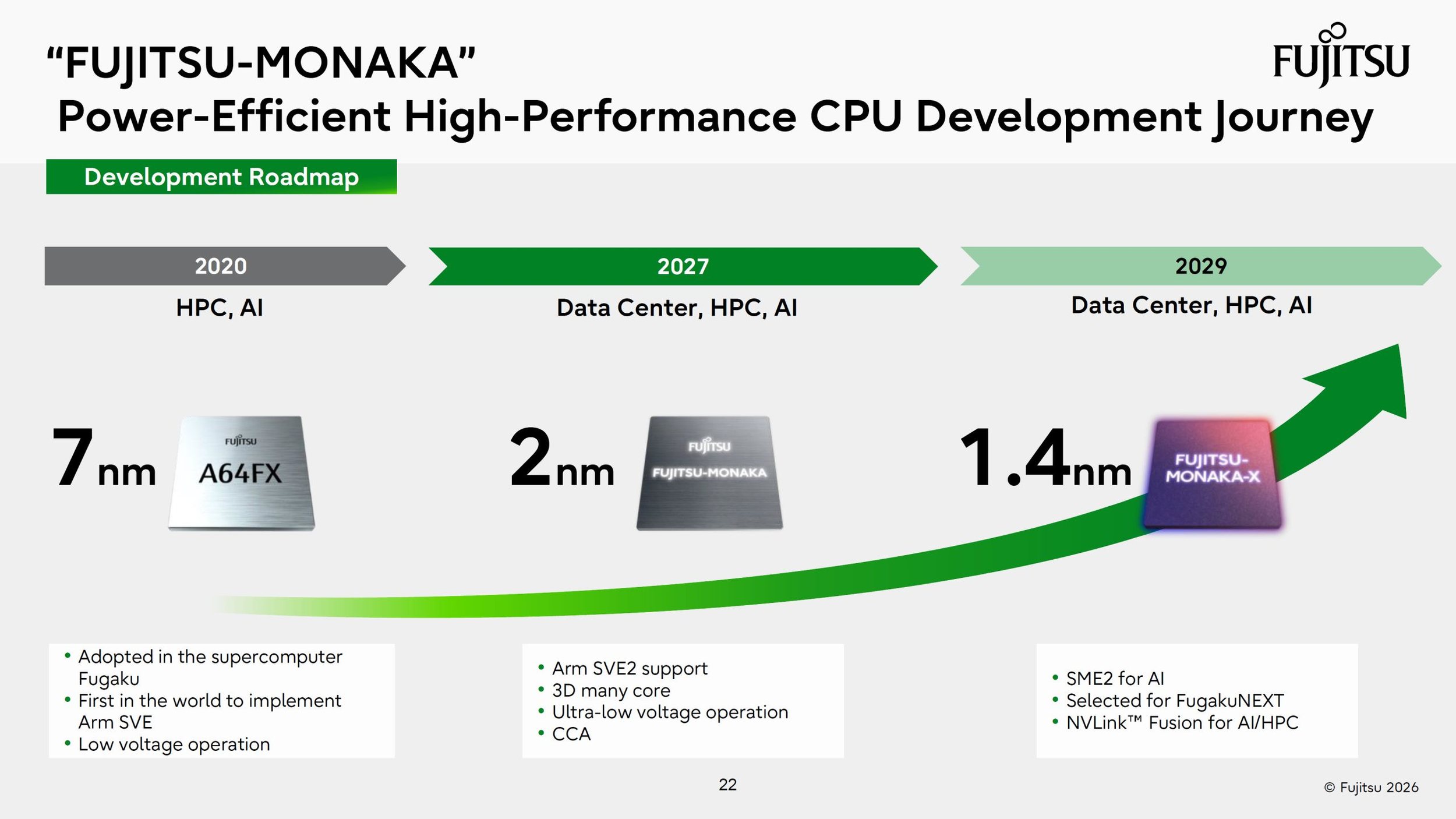
MONAKA X takes that philosophy further. More than 200 Arm cores, SME2, 1.4 nm technology and NVLink Fusion turn the processor into part of a tightly integrated AI and HPC system rather than an isolated server CPU. NVIDIA will still provide the enormous parallel acceleration required by modern AI, but Fujitsu clearly believes the CPU will become increasingly important for keeping those GPUs productive. FugakuNEXT could become one of the strongest demonstrations of that heterogeneous computing model when the architecture reaches deployment around the end of the decade.
Could Fujitsu's combination of 3D stacked CPU silicon and NVIDIA NVLink Fusion challenge the traditional x86 server model for future AI and HPC systems?
