
AMD Says Hybrid Bonded 3D DRAM Could Be 17x More Energy Efficient Than HBM
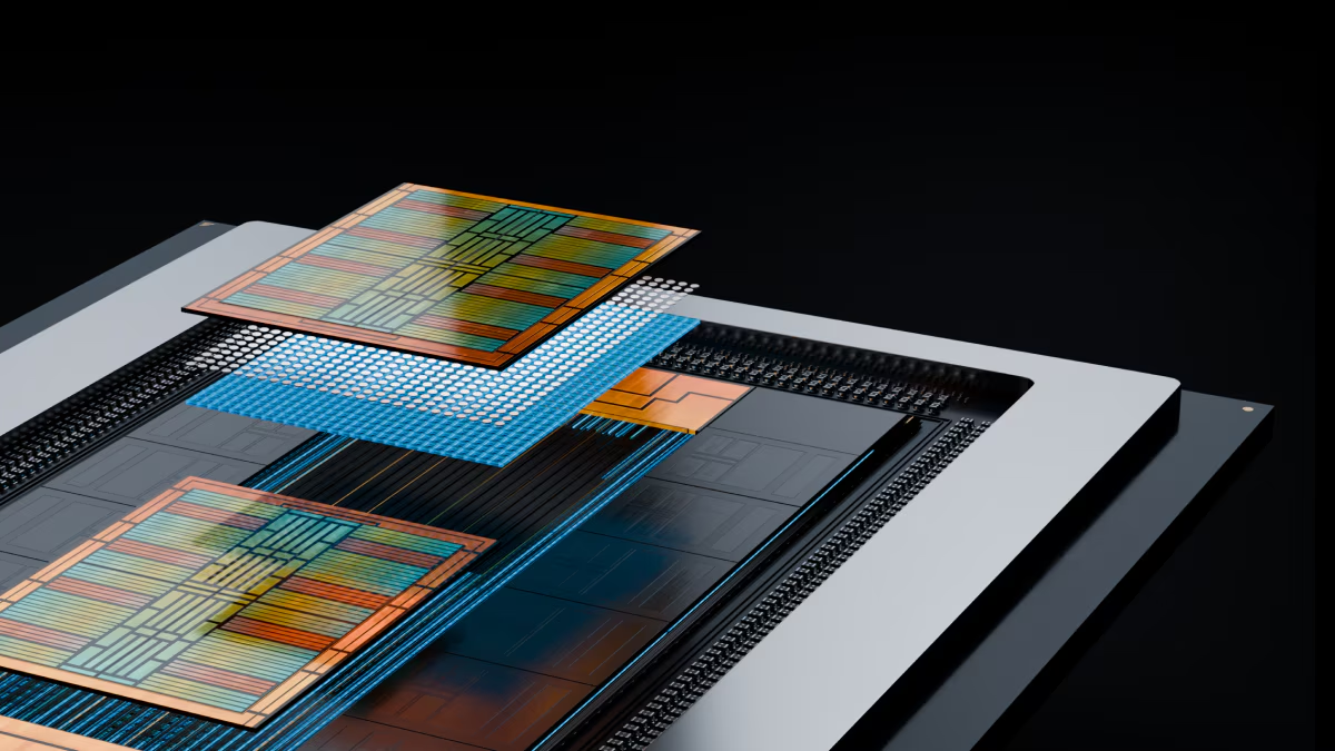
AMD is highlighting the enormous potential of hybrid bonded 3D DRAM as the AI industry searches for memory architectures capable of delivering more bandwidth without allowing power consumption to scale at the same rate. A presentation slide attributed to AMD and shared by technology investor Daniel Romero claims that hybrid bonded 3D DRAM could deliver as much as 17x better energy efficiency than conventional HBM using microbumps. The figure is significant, but it should currently be treated as an AMD attributed claim rather than an independently verified benchmark because detailed testing methodology has not been publicly released alongside the slide.
The underlying technology provides credible reasons for substantial efficiency improvements. Conventional HBM already stacks multiple DRAM dies vertically, but individual layers are generally connected through TSVs and microbump based interfaces. Microbumps introduce physical spacing, electrical resistance and capacitance between dies, while requiring additional materials and relatively large connection pitches compared with direct copper bonding.
Hybrid bonding removes those solder bumps and connects extremely small copper pads directly between adjacent silicon layers. AMD already uses this approach commercially with its 3D V Cache technology, where direct copper connections provide more than 15x the interconnect density and more than 3x the interconnect energy efficiency of AMD's comparison against microbump based 3D packaging. That does not independently validate the new 17x DRAM claim, but it demonstrates why AMD has substantial practical experience with the underlying packaging technology.
The potential becomes even greater when hybrid bonding is applied directly between logic and DRAM. Academic work on stacked embedded DRAM has demonstrated interfaces with extremely dense connections and energy consumption reaching approximately 0.88 pJ per bit, while newer research has demonstrated memory access energy around 0.66 pJ per bit using wafer level hybrid bonding. These published results independently support the broader argument that removing conventional high power memory interfaces can dramatically reduce the energy required to move data, although they do not reproduce AMD's specific 17x comparison.
$AMD says hybrid-bonded 3D DRAM is 17× more energy-efficient than HBM using microbumps pic.twitter.com/XMGgFZe0UY
— Daniel Romero (@HyperTechInvest) September 1, 2026
That difference matters because modern AI accelerators increasingly spend enormous amounts of power simply moving information between compute and memory. HBM solves much of the bandwidth problem by placing wide memory interfaces physically close to the accelerator, but every generation requires more bandwidth, more capacity and increasingly complex packaging. Micron has warned that AI compute performance is advancing faster than DRAM bandwidth, creating a memory wall where expensive accelerator silicon can spend substantial time waiting for data.
AMD is already experiencing this pressure directly with its current AI infrastructure. A single Instinct MI455X provides 432 GB of HBM4 and up to 19.6 TB/s of memory bandwidth, while an entire Helios rack combines 72 accelerators for approximately 31 TB of HBM4. As systems scale to these levels, reducing the energy consumed by every transferred bit becomes increasingly important because memory power eventually competes directly with compute power inside a fixed data center energy budget.
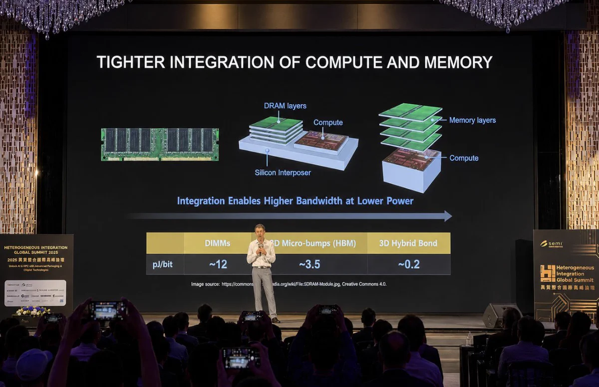
Hybrid bonded 3D DRAM could eventually take that integration even further by positioning memory extremely close to compute and removing more of the conventional interface overhead. Much smaller connection pitches can create dramatically wider interfaces operating at lower frequencies and voltages. Instead of pushing relatively fewer connections to increasingly high signaling speeds, designers can move data through thousands of extremely short vertical connections.
The problem is heat.
DRAM cells depend on tiny electrical charges that must remain stable between refresh cycles. Higher temperatures reduce retention time, forcing the memory to refresh more frequently and potentially increasing power consumption while reducing usable bandwidth. Academic research has demonstrated the relationship between thermal stress and declining DRAM retention characteristics, making thermal management particularly difficult when memory is placed directly beside or above extremely power dense AI compute silicon.
Hybrid bonding creates an additional manufacturing challenge because high quality copper connections traditionally require thermal treatment after the initial bonding process. Current industry processes can involve temperatures around 250°C to 350°C, while DRAM manufacturers would prefer substantially lower thermal budgets to protect sensitive memory structures. Semiconductor packaging researchers are therefore actively developing bonding processes below 250°C and potentially below 200°C.
Manufacturing precision is another barrier. Hybrid bonding requires exceptionally flat and clean surfaces because copper connections can be separated by only a few micrometers or less. Tiny particles, surface imperfections or alignment errors can create defective connections across an entire stacked structure. That becomes increasingly expensive when several valuable DRAM dies and a large compute die are being combined into one package.
These challenges explain why hybrid bonding has not immediately replaced microbump technology across commercial HBM. TrendForce expects the technology to become increasingly important as HBM moves toward taller stacks, particularly around future 20 layer HBM5 products, where conventional bonding becomes increasingly difficult because of package height, thermal resistance and connection density.
Memory manufacturers are already moving in that direction. SK hynix has verified a 12 die hybrid bonded HBM structure, although the company has not disclosed production yields and continues using established packaging methods while the new process matures. SK hynix is working to improve hybrid bonding yields before mass production, while Samsung is reportedly targeting broader hybrid bonded HBM production around 2029.
Interestingly, hybrid bonding can actually improve thermal characteristics once the final stack is successfully manufactured. A broad review of 3D HBM research found that optimized hybrid bonded structures can reduce junction to junction thermal resistance by between 22.8% and 47%, increase vertical thermal conductivity by as much as 3x and reduce overall stack height by more than 15%. The challenge therefore is not simply that hybrid bonding is thermally worse. It is that both the manufacturing process and the concentration of high power compute beside stacked DRAM create demanding thermal conditions that must be solved before very aggressive 3D integration can become commercially reliable.
The 17x figure is eye catching, but the architecture behind it is more important than the number itself. AMD has not yet provided enough public methodology to independently validate that specific efficiency comparison, so treating 17x as a guaranteed commercial advantage would be premature.
What is already clear is that conventional memory interfaces consume too much energy for the direction AI hardware is heading. Hybrid bonding attacks that problem by shortening connections, dramatically increasing interconnect density and eliminating much of the electrical overhead associated with microbumps and complex physical interfaces.
AMD also has a significant advantage in understanding this technology because 3D V Cache has already taken direct copper bonding from research into millions of commercial processors.
The real breakthrough will come when the semiconductor industry can apply similar integration to DRAM without compromising yield, retention or thermals. If that happens, future AI accelerators may no longer treat HBM as a collection of memory stacks sitting beside the processor. Memory and compute could effectively become different vertical layers of the same silicon system.
Could hybrid bonded 3D DRAM eventually replace conventional HBM for AI accelerators, or will thermal and manufacturing challenges keep the technology from reaching mass production?
