
Intel Says 14A Defect Reduction Is Fastest Since 22 nm as Foundry Push Intensifies

Intel is becoming increasingly confident in its next generation 14A manufacturing process, with CFO David Zinsner saying defect density is improving at the fastest pace the company has seen since its highly successful 22 nm technology launched in 2012. Speaking during Deutsche Bank's 2026 Technology Conference, Zinsner said 14A is tracking ahead of Intel's internal defect reduction target while internal product teams have already started designing chips around the process and external foundry customers are moving from evaluating technical data toward asking about available manufacturing capacity. The comments provide one of Intel's strongest signals yet that 14A could become the process technology on which its long term foundry recovery is built.
"14A, when you look at the defect density, is tracking better than the target curve we had for 14A."
— Quote by: David Zinsner, Intel CFO.
Zinsner also said Intel has not seen defects fall this quickly since 22 nm, which he described as one of the best manufacturing nodes Intel has ever produced. The comparison needs an important qualification. Intel is not claiming that 14A currently has the same defect density or production yield that mature 22 nm eventually achieved. The statement refers specifically to the rate at which defects are being reduced during development. Intel has not publicly disclosed the current 14A defect density or its internal target curve, meaning the absolute manufacturing quality of the process cannot yet be independently compared with competing advanced nodes.
That distinction matters because defect density is one of the fundamental variables influencing semiconductor yield. Fewer defects across a wafer generally increase the probability of producing functional chips, but final yield also depends on die size, design complexity, process maturity and other manufacturing factors. Intel's progress is therefore encouraging without proving that 14A has already achieved production ready yields.
The stronger signal may be what Intel's own product teams are doing. Zinsner said internal customers, which he jokingly described as probably Intel's most cynical group, are now designing products around 14A. Intel also disclosed through its latest SEC filing that multiple future Intel products are planned to use the node and that manufacturing expansion projects are already underway. External customers are simultaneously evaluating 14A for future products.
Customer discussions also appear to be advancing beyond early technical evaluation. Zinsner said CEO Lip Bu Tan and the Intel Foundry team are now meeting potential customers weekly, with conversations increasingly shifting toward questions about how much capacity Intel can provide and what future supply could look like. Intel previously expected external customers to begin making major supplier decisions during the second half of 2026 and first half of 2027.
This builds on the momentum previously covered when Intel 14A gained expanded Cadence support for design enablement and AI driven optimization. Cadence is helping Intel develop design flows, intellectual property and production ready process design kits, all of which are essential if 14A is going to become a genuine external foundry platform rather than another process primarily used by Intel's own products.
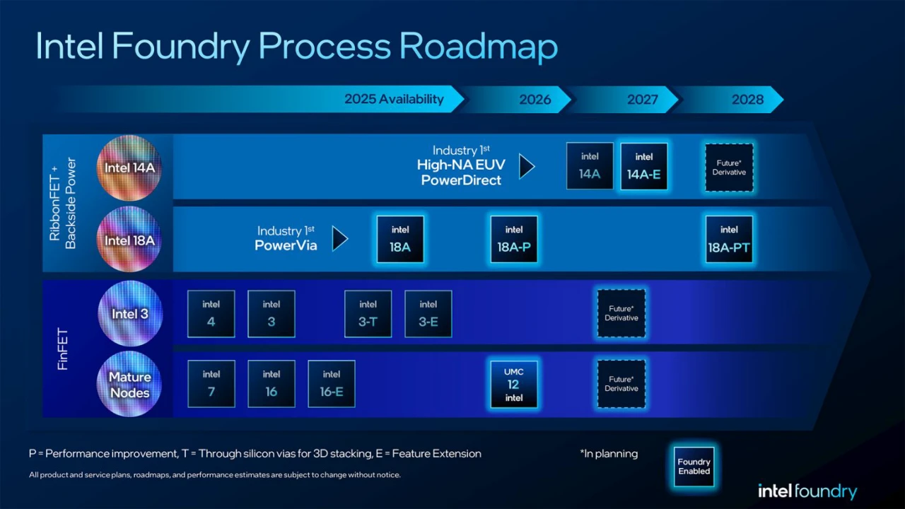
Intel expects the important 14A PDK 0.9 release to reach external customers in October 2026. Zinsner described the transition from PDK 0.5 to 0.9 as much more significant than the later move from 0.9 to the final 1.0 release. Intel currently plans to begin risk production during the second half of 2027, followed by high volume manufacturing in 2028. Those timelines mean semiconductor companies evaluating 14A today need to begin product design well before manufacturing reaches full scale.
Technically, 14A represents another major evolution beyond Intel 18A. According to Intel Foundry, the process introduces second generation RibbonFET gate all around transistors alongside PowerDirect backside power delivery. Intel claims 14A can deliver 15% to 20% higher performance at the same power, or 25% to 35% lower power at the same performance, alongside as much as 30% higher chip density compared with Intel 18A. Turbo Cells will also allow designers to selectively prioritize higher performance within critical CPU and GPU sections without applying the same power and area cost throughout an entire chip.
14A is also designed around High NA EUV lithography, an area where Intel has invested aggressively. High NA EUV provides greater lithographic resolution than conventional EUV and could reduce the number of patterning steps required for extremely dense semiconductor structures, although the equipment is substantially more expensive. This contributes to 14A becoming a more costly manufacturing technology than 18A, making external customer commitments particularly important for Intel to justify the required capital investment.
Intel's manufacturing strategy reflects that financial reality. Earlier in the turnaround, management said it would avoid building massive amounts of 14A capacity before customer demand became clearer. The company now appears more willing to increase investment after seeing stronger process execution and external interest. Zinsner said Intel raised 2026 capital spending from approximately $18 billion to $20 billion, while the company also completed a major capital raise to support future manufacturing, substrates and capacity requirements.
The node is especially important because Intel and TSMC are now targeting similar production windows for their next major process generations. TSMC says its own A14 technology will enter volume production in 2028, the same year Intel currently expects 14A high volume manufacturing. TSMC claims A14 will provide 10% to 15% higher performance at the same power or 25% to 30% lower power at the same performance compared with N2, alongside more than 20% additional logic density. TSMC also says its A14 yield development is currently ahead of schedule.
Matching production dates does not mean the 2 processes are directly equivalent. Process naming has not represented physical transistor dimensions for many generations, while performance, density, yields, libraries, packaging, pricing and customer requirements can differ significantly between foundries. However, having Intel and TSMC targeting advanced nodes for volume production during the same year puts Intel into a much more relevant competitive position than during the period when its manufacturing roadmap repeatedly slipped behind the Taiwanese foundry.
Intel still has much to prove. TSMC has an enormous advantage in manufacturing scale, customer trust and experience serving external chip designers. As previously discussed, TSMC Chairman C.C. Wei has argued that advanced manufacturing leadership cannot simply be recreated through capital investment, emphasizing the importance of production execution, customer qualification and reliable high volume capacity.
Intel's opportunity is therefore not simply beating TSMC on a specification sheet. It needs 14A to become predictable enough that companies are willing to place critical products into Intel factories. Recent reports have already pointed toward potential engagements involving major semiconductor and technology companies, although Intel has not publicly confirmed most of those companies as 14A production customers.
Intel comparing 14A development with 22 nm carries enormous symbolic weight. The 22 nm generation arrived during a period when Intel was considered the manufacturing leader of the semiconductor industry, long before delays around later nodes helped TSMC take that position. The important part is not nostalgia. It is that 14A appears to be improving faster than Intel expected while internal teams are beginning real product design and external customers are asking about capacity rather than simply studying process data.
That still does not equal a foundry victory. Intel has not disclosed absolute 14A defect density, major external customers remain largely unnamed and TSMC will have its own A14 technology entering production during the same 2028 window. But 14A increasingly looks like the node where Intel Foundry either becomes a credible long term alternative at the leading edge or proves how difficult rebuilding that position really is.
Do you think Intel 14A can finally make Intel Foundry a serious alternative to TSMC for major AI, CPU and GPU designs?
