
Intel Foundry Reportedly Secures Major AMD, NVIDIA and OpenAI Design Wins
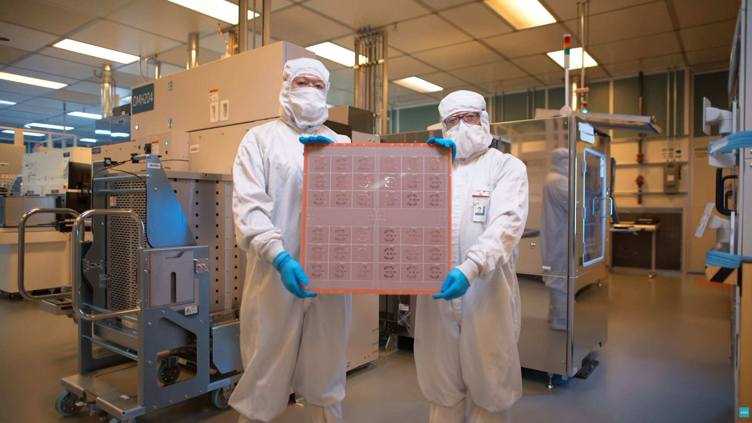
Intel Foundry has reportedly secured major customer engagements involving AMD, NVIDIA, Marvell, Microsoft, Micron, and OpenAI across its Intel 18A, Intel 18A P, and future Intel 14A process technologies. The claims originate from a KeyBanc Capital Markets report distributed through FactSet and subsequently circulated by industry sources including John Intel and Alex Intel. Some versions of the report also mention Apple and Meta, although Intel has not publicly confirmed most of these companies as manufacturing customers or disclosed which nodes, products, or components may be involved.
The reported wins would represent a significant validation point for Intel Foundry, particularly as semiconductor companies search for additional leading edge manufacturing and packaging capacity beyond TSMC. However, the term design win can cover several levels of engagement, including test chips, intellectual property blocks, secondary compute tiles, input and output dies, full processors, or advanced packaging services. It therefore remains unclear whether companies such as AMD, NVIDIA, and OpenAI have committed complete commercial products to Intel or are evaluating the technology for selected components.
Intel has confirmed that its base Intel 18A node entered production in 2025, using RibbonFET gate all around transistors and PowerVia backside power delivery. Intel’s regulatory filings state that the process entered high volume manufacturing during late 2025 and is being used for Core Ultra Series 3 products, including Panther Lake. The company expects Intel 18A and its derivatives to support several generations of future client and server processors while becoming its first major process family for external commercial foundry customers.
Intel 18A P entered risk production in June 2026 and remains compatible with the design rules used by standard Intel 18A, allowing customers to reuse existing intellectual property and development workflows. Intel claims that the enhanced process can provide 9% higher performance at the same power or 18% lower power at the same performance, alongside improved thermal resistance, reduced connection resistance, and additional transistor options. Our previous coverage of Intel 18A P entering risk production examines how these changes could make the node more attractive for AI accelerators, server processors, and high performance computing designs.
The analyst report estimates that Intel 18A yield has improved from approximately 65% during the previous quarter to more than 85%. Intel has not publicly confirmed that specific figure, and direct comparisons with reported yields for TSMC N2 or Samsung SF2 should be treated carefully. Yield percentages can vary substantially depending on die size, defect targets, test methodology, product maturity, and whether the figure refers to individual dies, complete wafers, or commercially usable products.
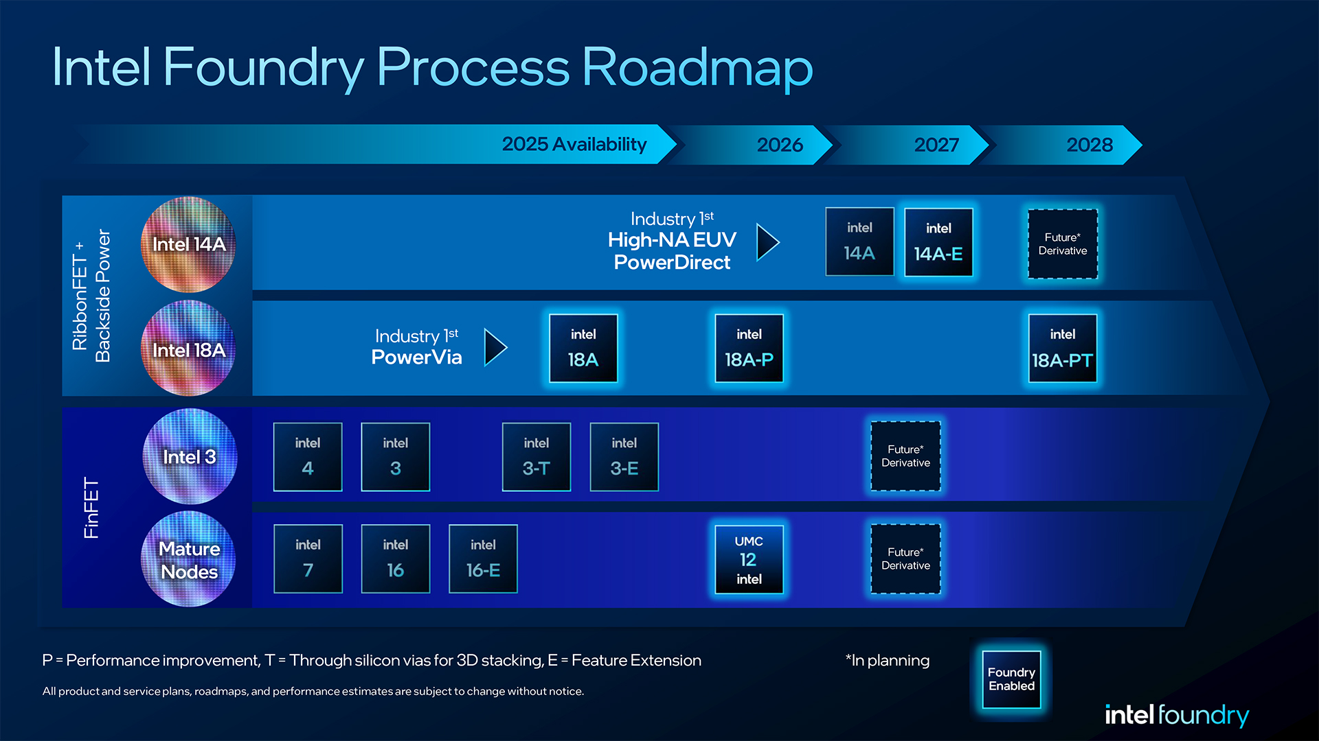
Intel 14A remains the company’s next major process platform and its first advanced node designed from the beginning around external foundry customers. Intel says the node will use RibbonFET 2 transistors and PowerDirect backside power delivery, targeting between 15% and 20% higher performance at the same power or between 25% and 35% lower power at the same performance compared with Intel 18A. It also targets up to 30% greater chip density. Intel is actively seeking major customers for the process, making any confirmed external commitment strategically important to the future economics of the node. Our earlier report on the expanding Intel 14A and Cadence partnership explains why design tools, reusable intellectual property, and customer support will be as important as transistor performance.
Intel’s advanced packaging business may be gaining momentum even faster. The same analyst information claims that EMIB T has achieved a 98% yield, improving from a previously reported level of approximately 90%. This figure has not been officially confirmed by Intel, but it would represent an important manufacturing milestone if accurate because advanced chiplet packages require extremely reliable connections across multiple logic dies, memory stacks, silicon bridges, and package substrates.
EMIB uses small silicon bridges embedded inside the package substrate to connect complex dies without requiring a full silicon interposer underneath the entire package. EMIB M adds metal insulator metal capacitors to the bridge, while EMIB T adds through silicon vias that can improve power delivery and enable larger heterogeneous designs. Intel says EMIB has been in mass production since 2017, while EMIB T was introduced in 2025 and is expected to scale more broadly from 2026. Intel recently created dedicated leadership for advanced packaging as it prepares EMIB T and hybrid bonding technologies for higher volume customer production.
The reported customer list would be transformative for Intel Foundry, but the most important word remains reportedly. Intel has publicly confirmed Microsoft as an Intel 18A customer, while the alleged engagements involving AMD, NVIDIA, OpenAI, Micron, Marvell, Apple, and Meta still require direct confirmation or visible commercial silicon before they can be treated as established production wins.
The EMIB T claim may ultimately be more significant than the headline node rumors. Advanced packaging has become one of the largest bottlenecks in AI infrastructure, and Intel does not need to manufacture every compute die to secure valuable business. It can package logic produced by different foundries, connect it with high bandwidth memory, and provide an alternative to capacity constrained packaging ecosystems.
Intel now appears to have the technology, domestic manufacturing footprint, and customer interest needed to become a credible second source. The next stage is execution. Yield consistency, pricing, production scale, software ready design tools, and predictable delivery will determine whether these reported engagements become long term customer relationships or remain evaluation programs.
Could advanced packaging become Intel Foundry’s fastest path back into the semiconductor leadership race, or will the company still need confirmed 18A and 14A production wins to challenge TSMC?
