
Intel 18A P Enters Risk Production With Power Boost And Dual Contact Transistor Design

Intel Foundry is putting more weight behind its advanced process roadmap with new details on Intel 18A P, the first performance enhancement in the Intel 18A family and one of the most important nodes for the company’s foundry ambitions. Shared during the 2026 VLSI Symposium, the update confirms that Intel 18A P has entered risk production, giving customers and ecosystem partners a clearer view of what the company expects to deliver beyond standard 18A.
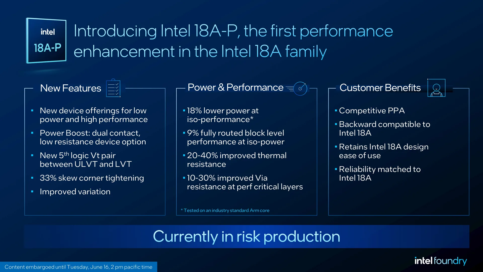
According to Intel Newsroom, Intel 18A P delivers 9% higher performance at the same power or 18% lower power at the same performance compared with Intel 18A. The node keeps the same core foundation of RibbonFET gate all around transistors and PowerVia backside power delivery, while adding new transistor, interconnect, thermal, and design technology improvements aimed at high performance computing, AI accelerators, mobile silicon, and data center products.
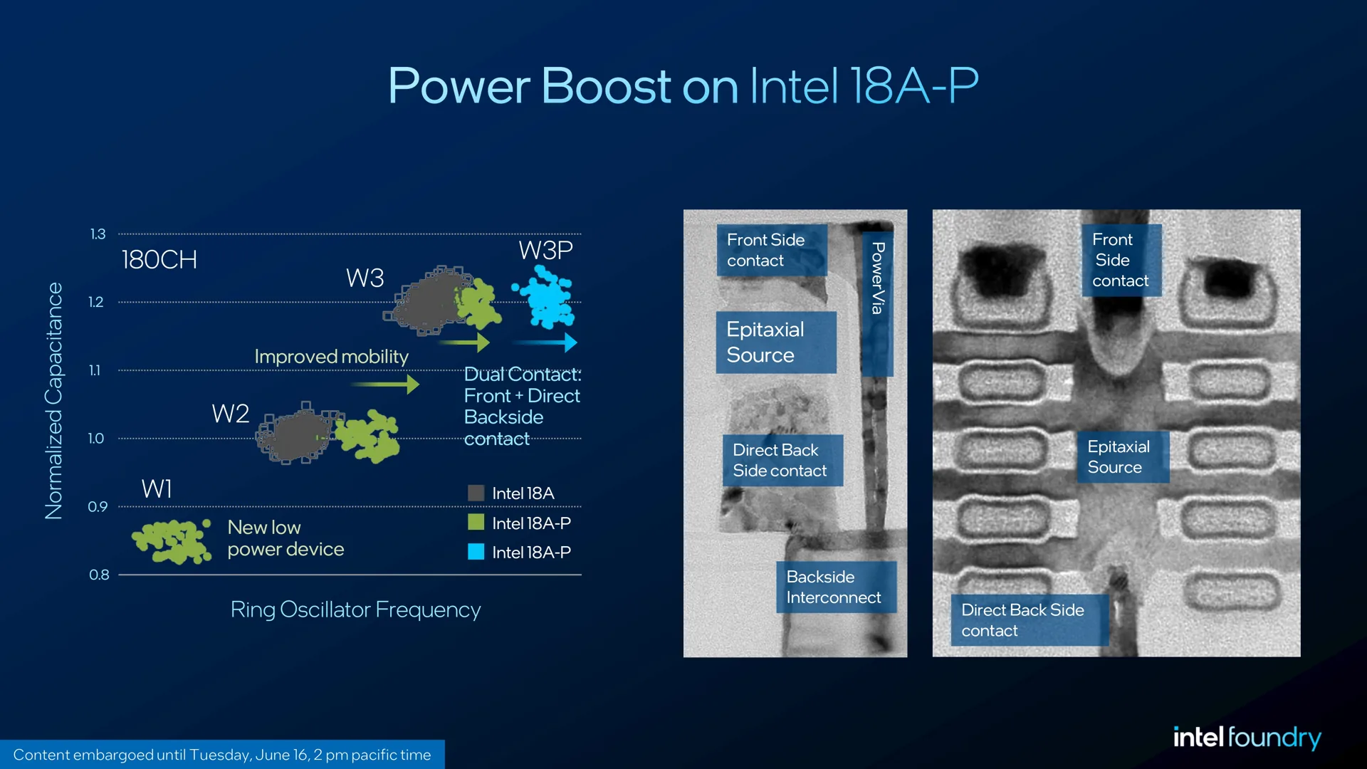
The most important new feature is Power Boost, which Intel describes as a new dual contact, low resistance transistor option. Instead of only relying on traditional front side contact behavior, Power Boost uses PowerVia backside power delivery to enable low resistance front side and direct backside contacts for both NMOS and PMOS transistors. The result is higher drive current and greater frequency at matched capacitance, allowing chip designers to push more speed from the same transistor footprint.

That matters because advanced chips are increasingly limited by power delivery, thermal behavior, and interconnect efficiency, not only transistor density. Modern AI processors and server CPUs need more performance inside strict power and area budgets, while customers also want predictable design reuse and lower migration friction. Intel 18A P tries to address that by staying design rule compatible with Intel 18A, which allows existing intellectual property and design flows to be reused more directly rather than forcing customers to rebuild everything from the ground up.
Intel’s VLSI 2026 technical session listing describes Intel 18A P as a performance enhanced RibbonFET gate all around technology with backside power delivery through PowerVia. The same listing says the gains come from new technology features, transistor performance enhancement, interconnect enhancement, and design technology co optimizations. In practical terms, Intel is trying to make 18A P feel less like a risky new platform and more like a stronger version of 18A that customers can adopt with less friction.
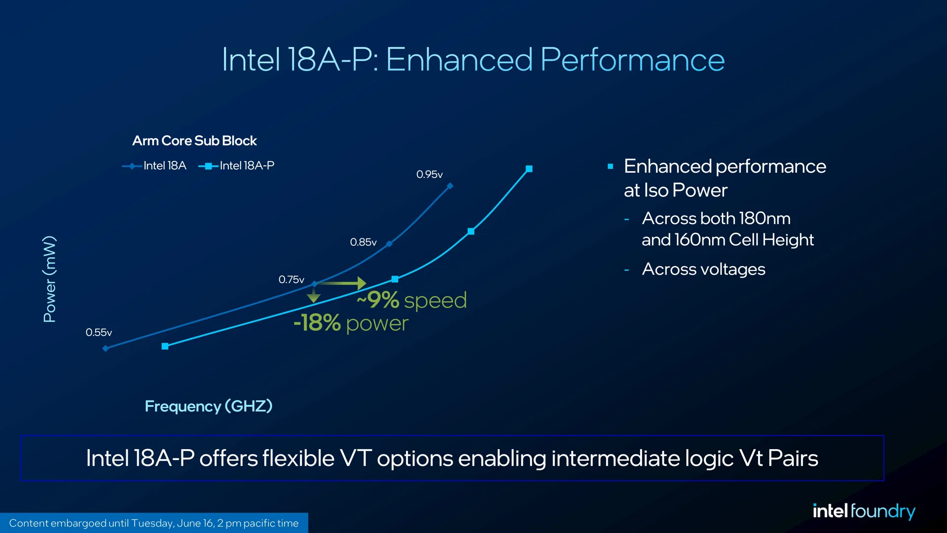
The node also brings thermal and resistance improvements that could become important for AI silicon. Intel says 18A P improves thermal resistance by 20% to 40% through materials and design innovations, while via resistance improves by 10% to 30% through geometry and materials optimization. Intel is also adding mobility enhancement through PMOS strain engineering, new low power and high performance transistor options, and a fifth logic Vt pair between ULVT and LVT, giving designers another tuning option when balancing speed, leakage, and power.
Intel 18A P keeps 2 cell heights, 180 nm and 160 nm, along with a contacted poly pitch of 50 nm. This helps preserve continuity with Intel 18A while expanding the performance and power design space. That continuity is strategically important for Intel Foundry because customer trust is not built only on peak performance claims. It also depends on tool flow stability, reusable IP, predictable yield learning, and confidence that the foundry roadmap can support real commercial products.
Backside power delivery remains a central part of Intel’s pitch. By moving major power routing to the back of the wafer, PowerVia reduces front side routing congestion and helps shorten signal paths. Intel says its work around gate all around transistors and backside power delivery enables 11% routed area reduction and a 10x reduction in dynamic voltage droop, with up to 6% frequency uplift or more than 15% dynamic power reduction compared with a comparable front side interconnect technology. That is a major reason Intel sees PowerVia not only as a node feature, but as a platform building block for future scaling.
The foundry message is also bigger than 18A P alone. Intel used VLSI 2026 to show longer range research in several directions, including 300 mm GaN and silicon integration for power management, CFET integration at a 45 nm gate pitch, and subtractive ruthenium interconnects with airgap integration. These are not immediate mass market node features, but they show where Intel is investing beyond today’s RibbonFET and PowerVia combination.
For AI hardware, this roadmap matters because the industry is fighting across several bottlenecks at once. Transistor scaling still matters, but so do power delivery, package level efficiency, advanced interconnects, thermal limits, and design flexibility. Intel’s 18A P is positioned as a foundry node that tries to improve several of those pressure points at once, especially for customers that need better frequency and power behavior without fully abandoning the 18A design ecosystem.
Intel also has internal product confidence tied to this node. At Computex 2026, Intel confirmed that Diamond Rapids, its next generation Xeon 7 platform, is planned for 2027 and will use Intel 18A P. That makes Diamond Rapids more than a server CPU update. It becomes one of the clearest signals that Intel intends to validate 18A P through its own high end data center roadmap while also presenting the node to external foundry customers.
This connects with previous coverage of how Apple and Google are reportedly evaluating Intel Foundry 18A P and EMIB. Even if customer adoption timelines remain uncertain, Intel’s messaging is becoming more consistent. The company wants 18A P to be seen not simply as a minor refresh, but as a more customer ready foundry node that can compete for future AI, client, mobile, and data center designs.
The challenge is execution. Intel has strong technology talking points with RibbonFET, PowerVia, Power Boost, improved thermals, and design rule compatibility, but the foundry market rewards consistent delivery more than slide level ambition. TSMC remains the dominant external foundry for leading edge silicon, and Intel still needs to prove yield maturity, design ecosystem readiness, customer support, and volume manufacturing reliability at a competitive level.
Intel 18A P looks like one of the most important process updates in the company’s foundry reset. The technical improvements are meaningful, especially Power Boost and the thermal resistance gains, but the larger story is trust. Intel is trying to show customers that 18A was the foundation, 18A P is the customer focused refinement, and 14A is the next major leap. If Intel can turn that roadmap into real customer silicon, 18A P could become a key milestone in the company’s attempt to rebuild itself as a serious leading edge foundry competitor.
Do you think Intel 18A P can help Intel Foundry win more major AI and data center customers, or does Intel still need 14A to truly challenge TSMC?