
Intel and SoftBank’s ZAM Memory Targets the High Bandwidth AI Market With Bandwidth That Could Reach More Than Double HBM4
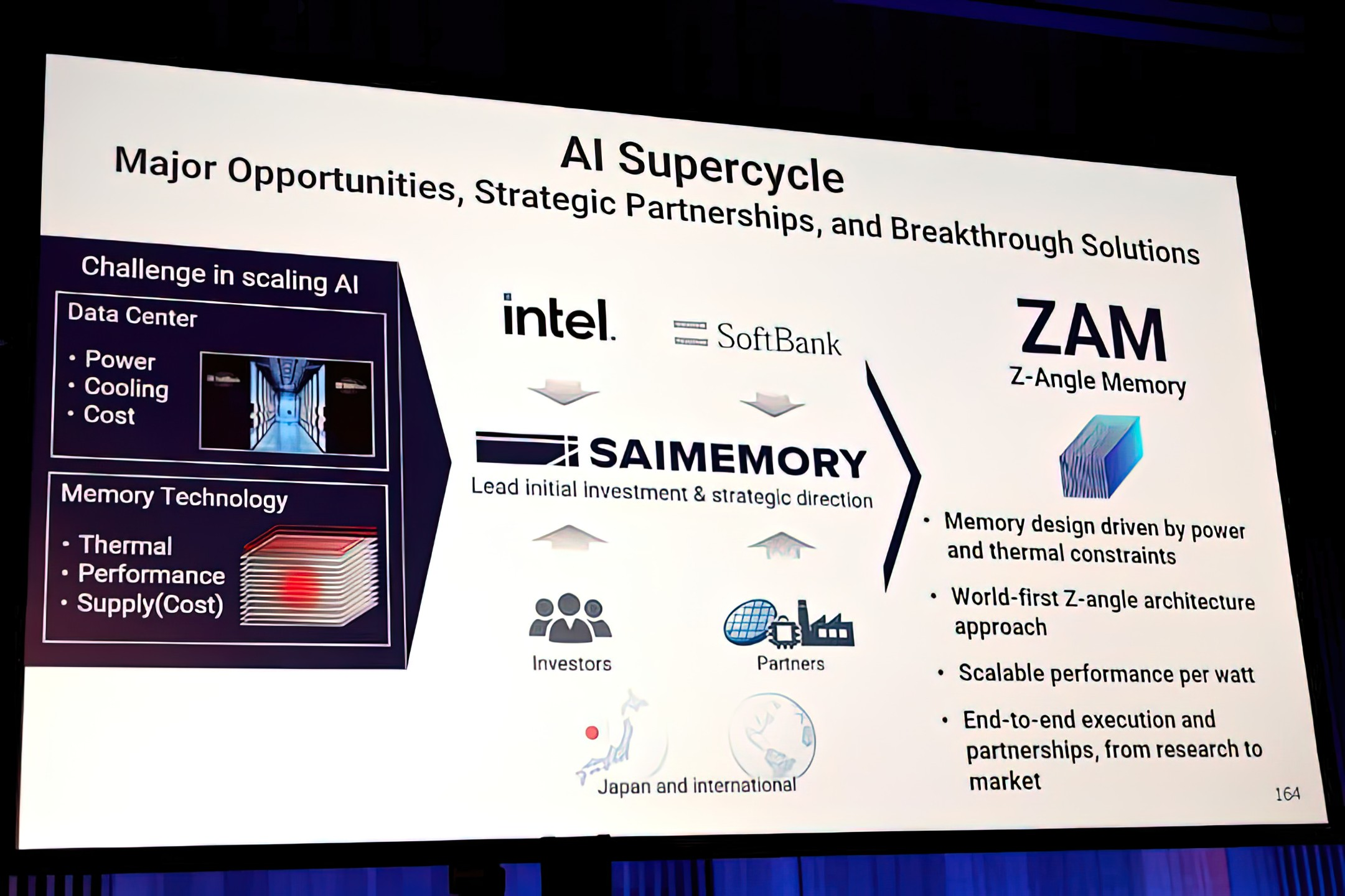
Intel and SoftBank backed SAIMEMORY are pushing a bold new memory concept called Z Angle Memory, or ZAM, into the spotlight, and the early technical preview suggests it could become one of the most ambitious challengers yet to conventional HBM in AI infrastructure. According to SAIMEMORY, the project is being developed as a next generation memory technology focused on high capacity, high bandwidth, and low power consumption, with commercialization targeted for fiscal 2029 after prototype work planned for fiscal 2027.
That timeline alone makes ZAM a long range play rather than an immediate product threat, but the performance targets are what make this project especially interesting. A technical preview for the 2026 VLSI Symposium describes a SAIMEMORY and Intel paper covering a multiple wafer, 9 layer, extreme thin 3D high bandwidth DRAM architecture that offers about 0.25 Tb/s per mm² at low data transfer power. The same preview notes an 8 stacked cube design with 1.125GB per die and 13.7K via in one TSV arrays per die, giving the first real glimpse at how dense and aggressive the architecture is intended to be.
Those numbers imply a very serious bandwidth target. Based on the figures tied to the symposium preview and repeated in industry coverage, a single ZAM stack could deliver roughly 5.3TB/s of bandwidth. That matters because standard HBM4 is widely described as delivering about 2.048TB/s per stack through a 2048 bit interface at 8 Gb/s, while HBM4E is expected to push that higher to 4.096TB/s at 16 Gb/s. In other words, if ZAM reaches its stated goals, it would not just challenge HBM4, it could move beyond even the first wave of HBM4E class throughput on a per stack basis.
Intel ZAM is achieving 2x speeds of HBM4 and matching future speed of HBM4E
— Alex (@Alex_Intel_) May 2, 2026
Except ZAM is using a cooked up PSMC 20nm DRAM node thats 10 years old (speculation but PSMC is apart of the paper and 20nm is the best they have)
Great resources in quote below for patents and paper https://t.co/tA9zc24zKA
The architectural approach is part of what makes ZAM stand out. The VLSI preview describes a fusion bonded via in one structure using extreme thin silicon in each DRAM layer, with every metal routing layer in the stacked cube directly linked to the TSV bus for better signal and power integrity. That is very different from the packaging and interconnect assumptions most people associate with today’s HBM products. The project is also tied to research around low power data transfer, and RIKEN describes ZAM itself as a next generation memory technology characterized by high capacity, high bandwidth, and low power consumption.
This is also not just a two company experiment anymore. SAIMEMORY and Intel formally announced their collaboration in February, and RIKEN later confirmed both an investment in SAIMEMORY and participation in a Japanese government supported research effort titled “Development of High Density, High bandwidth, Low Power ZAM.” That broader backing is important because it suggests ZAM is being treated as a serious strategic memory project rather than a small lab demonstration.
From a market perspective, the pitch is clear. HBM remains the dominant memory solution for AI accelerators and high end compute, but it also comes with well known challenges around power, thermals, packaging complexity, and scaling cost. ZAM is being framed as an attempt to attack exactly those pressure points while still offering the kind of capacity and bandwidth AI servers will need later in the decade. If that works, Intel and SoftBank could be positioning ZAM as a next generation memory layer for training and inference systems where both memory bandwidth and energy efficiency have become critical bottlenecks.
Still, this is where the article needs a reality check. ZAM is promising, but it is not proven in the market. The current information comes from collaboration announcements, institutional backing, and an advanced symposium preview, not from a shipping product or a production scale benchmark against real HBM based accelerators. There are still open questions around yields, manufacturing scale, ecosystem readiness, controller integration, packaging compatibility, and whether developers and system makers would adopt an entirely new memory stack in volume. Even strong technical ideas can struggle if they arrive late, cost too much, or fail to fit existing AI platform roadmaps.
That said, the concept is undeniably one to watch. The combination of high bandwidth density, stacked 3D structure, low power ambitions, and strong institutional support gives ZAM more substance than many early memory ideas ever receive. If Intel, SoftBank, and SAIMEMORY can move from research validation to practical deployment by the end of the decade, ZAM could become one of the most disruptive memory stories in the AI hardware market.
Would you trust a new memory standard like ZAM to challenge HBM in real AI systems, or do you think the market will stay locked to existing HBM suppliers for the rest of the decade?