
NVIDIA Reportedly Pulls Co Packaged Optics Forward to 2028 With Feynman, Accelerating a Key AI Interconnect Shift
NVIDIA appears to be moving much faster on co packaged optics than many in the industry expected. According to a new report from Nikkei Xtech, the company has effectively pulled commercial co packaged optics adoption forward by about 5 years, with the first GPU side implementation now expected to arrive in 2028 alongside its Feynman generation. If that timeline holds, it would mark a major roadmap acceleration for silicon photonics inside AI infrastructure, especially as rack scale systems continue to expand in size, bandwidth demand, and physical distance.
The broader significance is easy to understand. Co packaged optics replaces more of the traditional copper based signal path with optical links, allowing much higher bandwidth and better reach while reducing some of the power and signal integrity issues that become harder to manage as AI clusters grow. NVIDIA has already described its long term AI infrastructure strategy around much larger scale systems, and the newly formed OCI MSA says its goal is to establish open, interoperable optical interconnect specifications for AI scale up. That consortium includes major names such as NVIDIA, AMD, Broadcom, Meta, Microsoft, and OpenAI, showing that the industry is already treating optical interconnect as a serious next phase for AI networking rather than a distant side experiment.
What makes the new report stand out is the difference versus NVIDIA’s earlier tone. In March 2025, Reuters reported Jensen Huang saying that co packaged optical technology was not yet reliable enough for NVIDIA’s mainline GPU deployment and that broader use would have to wait, with optics initially limited to networking chips rather than GPU compute products. That is why the current 2028 Feynman target matters so much. It suggests NVIDIA has moved from caution around GPU side optics to active roadmap integration within just about a year.
At GTC 2026, NVIDIA officially confirmed several of the big building blocks around that future platform. The company said that Feynman would follow Vera Rubin as its next major architecture, that it would pair with a new CPU called Rosa, and that the roadmap includes optical NVLink and new networking components in that same era. NVIDIA’s own GTC 2026 coverage specifically names Rosa as the CPU that will accompany Feynman, while third party roadmap reporting from the event highlights optical NVLink, BlueField 5, and next generation switching as part of the 2028 stack.
The optics angle is also reinforced by the networking roadmap around Feynman. Reporting based on GTC 2026 says NVIDIA’s 2028 platform will include NVLink 8 with co packaged optics, alongside new Ethernet and DPU components. The Next Platform also noted that NVIDIA had already put co packaged optics into its Rubin generation Spectrum 6 Ethernet plans, which makes Feynman look less like a sudden one off jump and more like the next step in a staged optical transition that begins in networking and then expands further into the compute fabric.
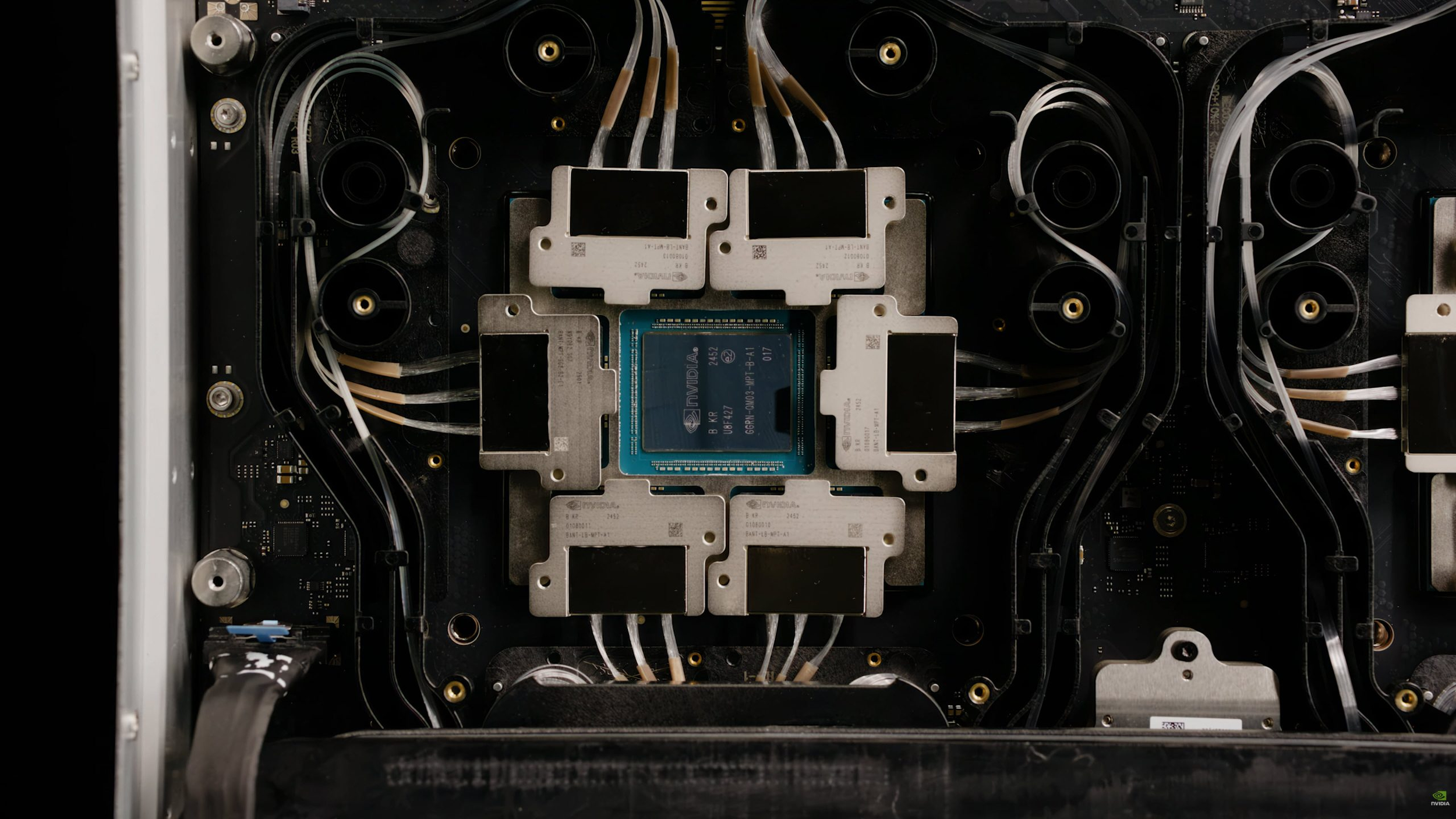
Another important piece is packaging. Coverage following GTC 2026 says NVIDIA’s Feynman GPUs are expected to use die stacking, while the Nikkei linked discussion suggests Intel could be involved through advanced packaging capability. NVIDIA has not publicly confirmed Intel Foundry participation for Feynman in the official material I checked, so that part should still be treated as report driven rather than confirmed fact. What is confirmed is that NVIDIA is positioning Feynman as a major architectural transition point rather than a routine annual refresh.
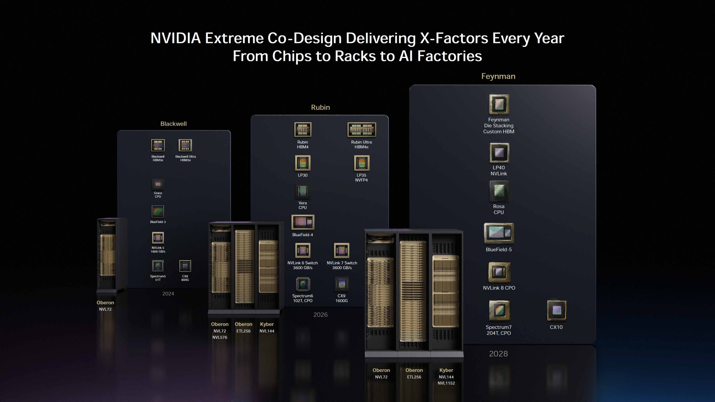
The memory side is equally interesting. GTC 2026 reporting shows Rubin using HBM4 and Rubin Ultra using HBM4E, while Feynman is associated with custom HBM rather than a standard next step naming convention. That wording has fueled speculation that NVIDIA may be preparing either a highly customized HBM4E derivative or an early custom path toward HBM5 class packaging. NVIDIA has not publicly detailed what that custom HBM means yet, but the fact that it is being called out separately suggests memory will be a major differentiator for the 2028 platform.
The reason all of this matters is scale. AI systems are no longer just about the speed of a single GPU. They are increasingly limited by how effectively thousands of accelerators can be linked together across racks and potentially across much larger physical footprints. Optical links are attractive because they can carry very high data rates over longer distances than copper while helping reduce some of the thermal and signal challenges that emerge at scale. If NVIDIA really is bringing GPU linked co packaged optics to market in 2028, then Feynman may end up representing one of the most important infrastructure shifts since NVLink itself became central to its AI platform story.
For now, the safest conclusion is this: NVIDIA has officially shown a 2028 Feynman platform with Rosa CPU and optical interconnect elements, while the claim that co packaged optics has been pulled forward by 5 years comes from report coverage rather than direct official wording. Even so, the roadmap direction is clear. NVIDIA is no longer talking about optics as a far off possibility. It is now putting optical scale up much closer to the center of its future AI factory design.
Do you think co packaged optics will be the next true turning point for AI hardware, or will advanced copper and packaging still carry the market longer than expected?