
TSMC CoWoS Yield Surpasses 98% as AI Packaging Scales Toward Massive 14 Reticle Designs
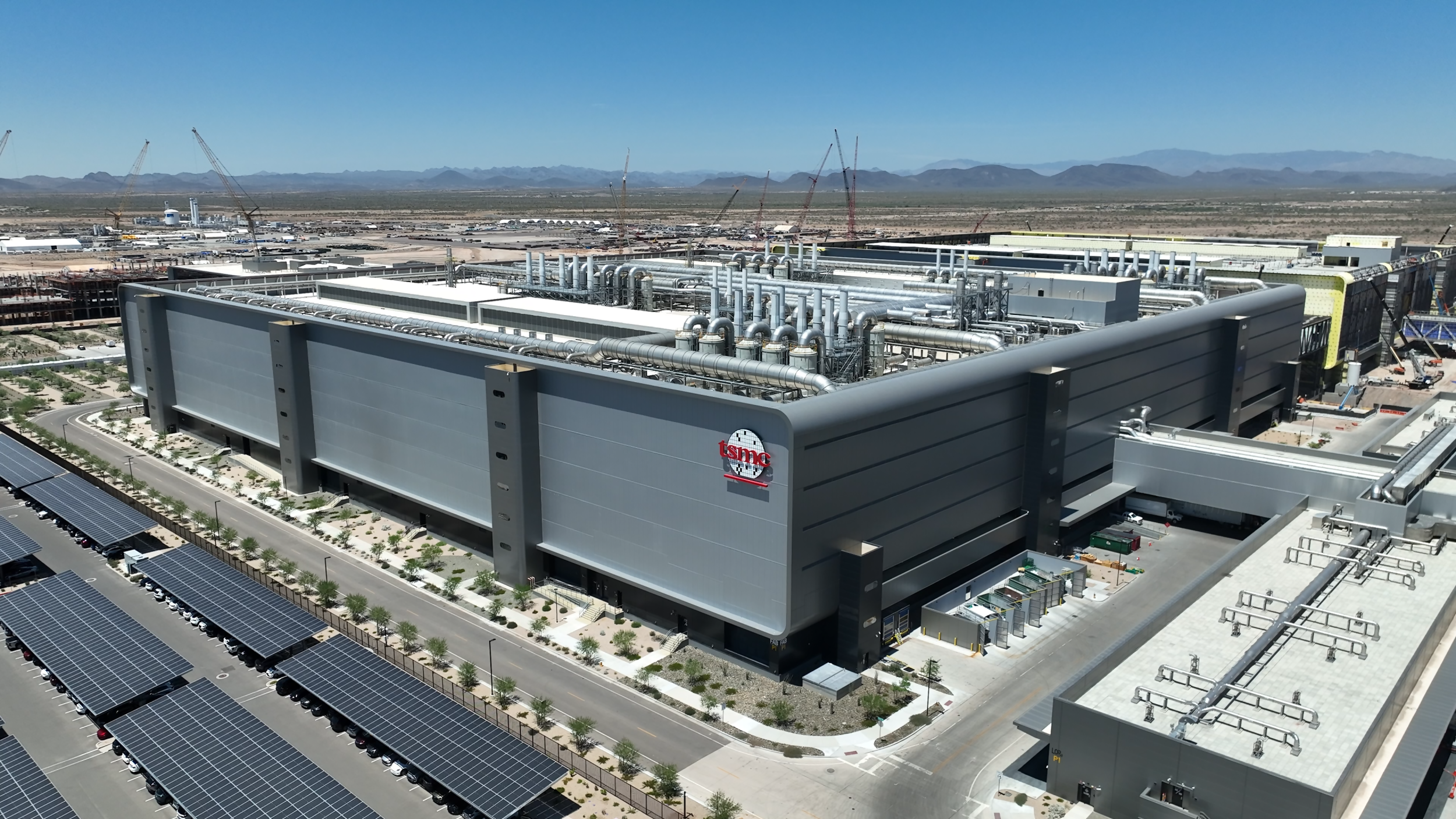
TSMC has reached another major milestone in advanced semiconductor packaging, with its latest 5.5 reticle size CoWoS technology achieving yields consistently above 98% across multiple AI customer products, while some products have already reached 99%. TSMC Vice President of Advanced Packaging Technology and Service Ho Chun disclosed the figures during the 2026 OCP APAC Summit, confirming that the 5.5 reticle generation has entered high volume production as demand for increasingly larger AI processors continues to accelerate. According to Taiwan's Economic Daily, TSMC has also been expanding CoWoS capacity at close to 2 times per year during the past 3 years and now operates 10 advanced packaging facilities, bringing available capacity increasingly close to customer demand, although supply has not yet completely caught up.
"We are already in mass production of the 5.5 reticle size CoWoS, and yields for multiple AI customer products are consistently above 98%, with some reaching 99%."
— Quote by: Ho Chun, TSMC Vice President of Advanced Packaging Technology and Service
The achievement is especially significant because CoWoS packages are becoming dramatically larger and more complicated as AI processors combine multiple compute dies, chiplets and HBM stacks inside a single package. Increasing package area introduces additional challenges involving interconnect density, thermal expansion, substrate deformation, power delivery and the probability that manufacturing defects affect the finished product. Maintaining yields above 98% at the 5.5 reticle scale therefore demonstrates how mature TSMC's packaging process has become. TSMC describes CoWoS as a core 2.5D packaging platform for AI and high performance computing, allowing multiple SoCs and HBM stacks to operate together through extremely dense interconnections.
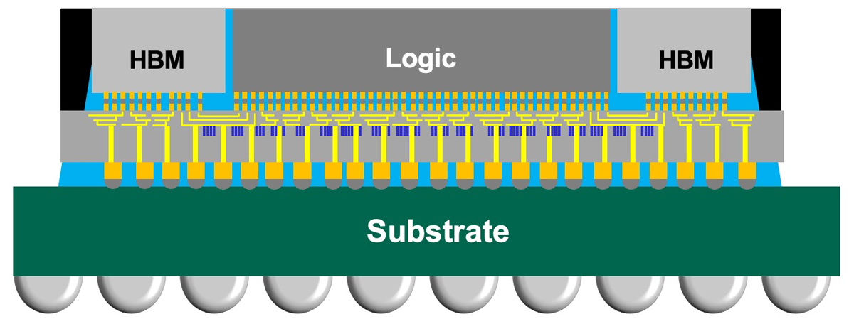
TSMC is already preparing considerably larger generations. At its 2026 North America Technology Symposium, the company confirmed that 5.5 reticle CoWoS had entered production and outlined a future 14 reticle implementation capable of combining approximately 10 large compute dies with 20 HBM stacks in a single package. TSMC's April roadmap placed 14 reticle production in 2028 followed by designs exceeding 14 reticles in 2029, while Ho's latest OCP APAC comments described the company's progression toward the 14 reticle scale through 2029 as development cycles accelerate to approximately 1 new CoWoS generation every year.
The rapid expansion reflects how advanced packaging has become as important to modern AI accelerators as leading edge transistor technology itself. NVIDIA GPUs and custom AI processors increasingly require multiple compute dies and large quantities of HBM, making CoWoS a critical connection between silicon production and usable AI accelerators. This remains visible with NVIDIA GB300 wafers manufactured at TSMC Arizona, where wafer fabrication can occur in the United States while critical CoWoS packaging remains concentrated in Taiwan. TSMC is simultaneously investigating longer term packaging materials, including glass based approaches for future CoWoS generations, as organic substrates face increasing mechanical and scaling challenges from massive AI packages.
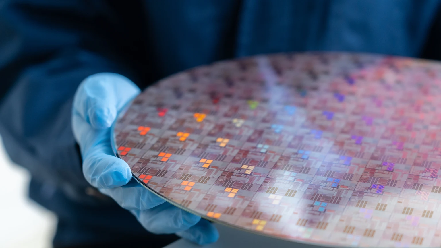
Ho also highlighted one of the fundamental advantages of chiplet based designs. Instead of manufacturing every function on a single enormous leading edge die, companies can divide processors into specialized dies manufactured using different process nodes and then integrate them through advanced packaging. TSMC can additionally use electrical characteristics and performance data to pair individual dies more effectively before packaging, improving consistency and potentially recovering silicon that might otherwise be unsuitable for certain products. With AI customers demanding larger processors at increasingly aggressive development cycles, TSMC is effectively transforming CoWoS from a packaging technology into a core system level scaling platform.
A 98% to 99% yield on packages this complex is arguably as important as another transistor density improvement. AI hardware is moving beyond the era where performance gains can come primarily from building a larger monolithic GPU. Future accelerators will increasingly depend on combining compute dies, HBM, I/O and specialized silicon into enormous packages, making packaging yield a direct factor in production cost and available AI capacity. TSMC achieving near 99% yields at 5.5 reticle scale gives it an enormous manufacturing advantage while competitors such as Intel push alternatives including EMIB. The next challenge will be maintaining that level of manufacturing efficiency as CoWoS moves toward packages capable of carrying 10 compute dies and 20 HBM stacks.
As AI processors become increasingly dependent on chiplets and HBM, do you think advanced packaging will become a bigger competitive advantage than the semiconductor process node itself?
