
NVIDIA’s First GB300 Wafers Emerge From TSMC Arizona but CoWoS Packaging Remains in Taiwan
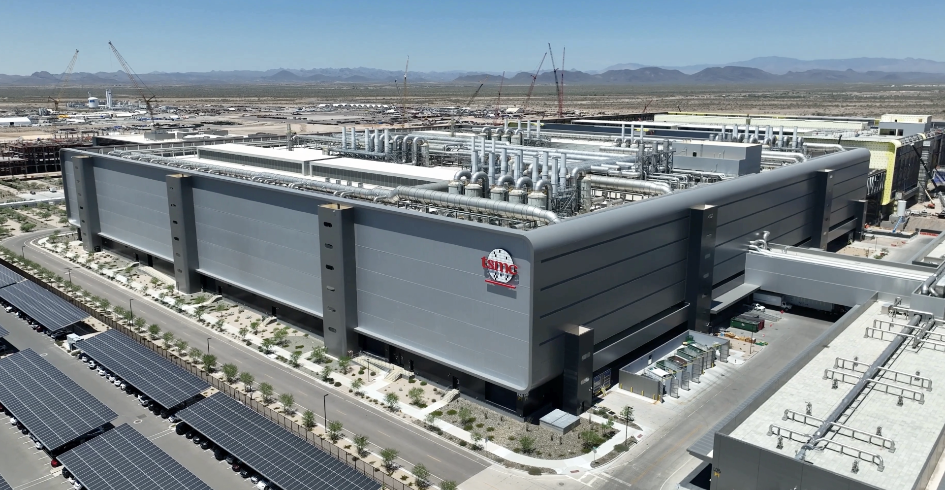
NVIDIA and TSMC have reached another major milestone in the effort to build advanced artificial intelligence chips in the United States, with the first NVIDIA GB300 Blackwell Ultra wafer reportedly completed at TSMC’s Fab 21 facility in Phoenix, Arizona.
According to the Commercial Times report, TSMC manufactured the GB300 silicon using its 4 nm process at the first Arizona fab. NVIDIA has separately confirmed that its Blackwell wafers are now being manufactured in volume at TSMC’s Phoenix facility, providing official confirmation that Arizona has progressed beyond early samples into commercial AI chip production.
However, the Arizona output should not yet be described as a completely manufactured American GPU. Fab 21 currently produces the silicon wafers, but the completed dies must still be transported to Taiwan for CoWoS advanced packaging before they can be integrated with High Bandwidth Memory and prepared for system assembly.
CoWoS is a critical part of NVIDIA’s AI accelerator supply chain because it combines the GPU dies, supporting chiplets, and HBM stacks inside an extremely dense package. Without this stage, the wafer produced in Arizona cannot become a functional GB300 accelerator or enter an NVL72 system.
The achievement therefore highlights both the progress and the remaining limitation of semiconductor localization in the United States. TSMC can now manufacture advanced NVIDIA logic in Arizona, while Foxconn is expanding AI server production in Houston and Wistron has opened a $700 million facility in Fort Worth that is already producing GB300 Grace Blackwell Ultra Superchips. The final missing component is large scale domestic advanced packaging.
TSMC intends to address that gap through 2 advanced packaging facilities planned for Arizona. After previously committing $165 billion to its United States expansion, the company announced another $100 billion investment in July 2026, bringing the total planned commitment to $265 billion. The broader project includes 6 wafer fabs, 2 advanced packaging facilities, and a research and development center.
The expansion builds on previous coverage of TSMC’s $265 billion Arizona investment, which also highlighted that constructing fabrication facilities in the United States can cost between 4 and 5 times more than comparable projects in Taiwan.
TSMC’s official Arizona roadmap currently places N3 volume production at its second fab during the second half of 2027. Its third fab is expected to introduce N2 and A16 technologies by the end of the decade. TSMC has not confirmed that N2 or A16 production will begin in Arizona during 2028, although additional fabs and packaging capacity will follow according to customer demand and construction progress.
Once CoWoS and related SoIC packaging capabilities become available in Arizona, NVIDIA could potentially keep significantly more of its Blackwell and future Rubin production process inside the United States. This would connect wafer fabrication in Phoenix with advanced packaging in Arizona and AI system manufacturing in Texas.
The milestone also reinforces why advanced packaging remains one of the semiconductor industry’s most important bottlenecks. TSMC’s 2 nm, 3 nm, and CoWoS expansion, producing more accelerator wafers is only useful when enough packaging capacity exists to combine those dies with memory and turn them into deployable AI hardware.
The first Arizona manufactured GB300 wafers represent genuine progress, but they also demonstrate why semiconductor independence cannot be measured by wafer production alone.
Modern AI accelerators are complete systems built through several highly specialized stages. The logic die may come from Arizona, but packaging expertise, HBM integration, substrates, testing, boards, cooling, and rack assembly remain equally important.
TSMC’s planned packaging facilities could eventually close the most significant gap in the American AI manufacturing chain. Until they enter volume production, the United States will have domestic Blackwell wafer capacity, but not a completely domestic path from silicon to finished accelerator.
For NVIDIA, the immediate benefit is geographic diversification. For the United States, the larger victory will arrive when a GB300 or Rubin accelerator can move from wafer fabrication through advanced packaging and final system assembly without crossing the Pacific.
Does producing Blackwell wafers in Arizona meaningfully strengthen the United States semiconductor supply chain, or will Taiwan remain indispensable until CoWoS packaging is fully localized?
