
Intel 18A P and 14A Gain Full Cadence Certification as Foundry Push Targets TSMC’s Ecosystem Advantage
Intel Foundry has secured another important component of its advanced manufacturing strategy after Cadence certified its broad portfolio of artificial intelligence driven design tools, reference flows, and solutions for Intel 18A P and Intel 14A.
According to the official Cadence announcement, the certification is based on the latest Intel Foundry process design kits and gives chip designers a validated path for developing artificial intelligence, high performance computing, mobile, and advanced system on chip products using Intel’s next generation manufacturing technologies.
The certified flows cover the major stages required to transform a chip architecture into a manufacturable design, including synthesis, placement and routing, timing analysis, power signoff, physical verification, reliability validation, and analog and custom design. Cadence and Intel have jointly tuned these tools around the manufacturing rules and characteristics of Intel 18A P and Intel 14A, reducing the risk that customers will need to build or validate critical parts of the workflow independently.
This certification is especially important because a competitive process node requires more than strong transistors. Customers also need mature software, validated intellectual property, accurate design rules, packaging support, and signoff tools that can identify manufacturing and reliability problems before a design reaches production.
"As designers look for new ways to differentiate their products in this exciting era of AI, Intel Foundry's collaboration with ecosystem partners such as Cadence will help our customers turn their most ambitious ideas into reality."
— Quote by: Shawn Han
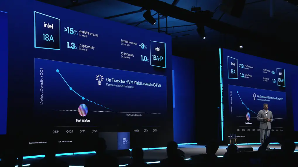
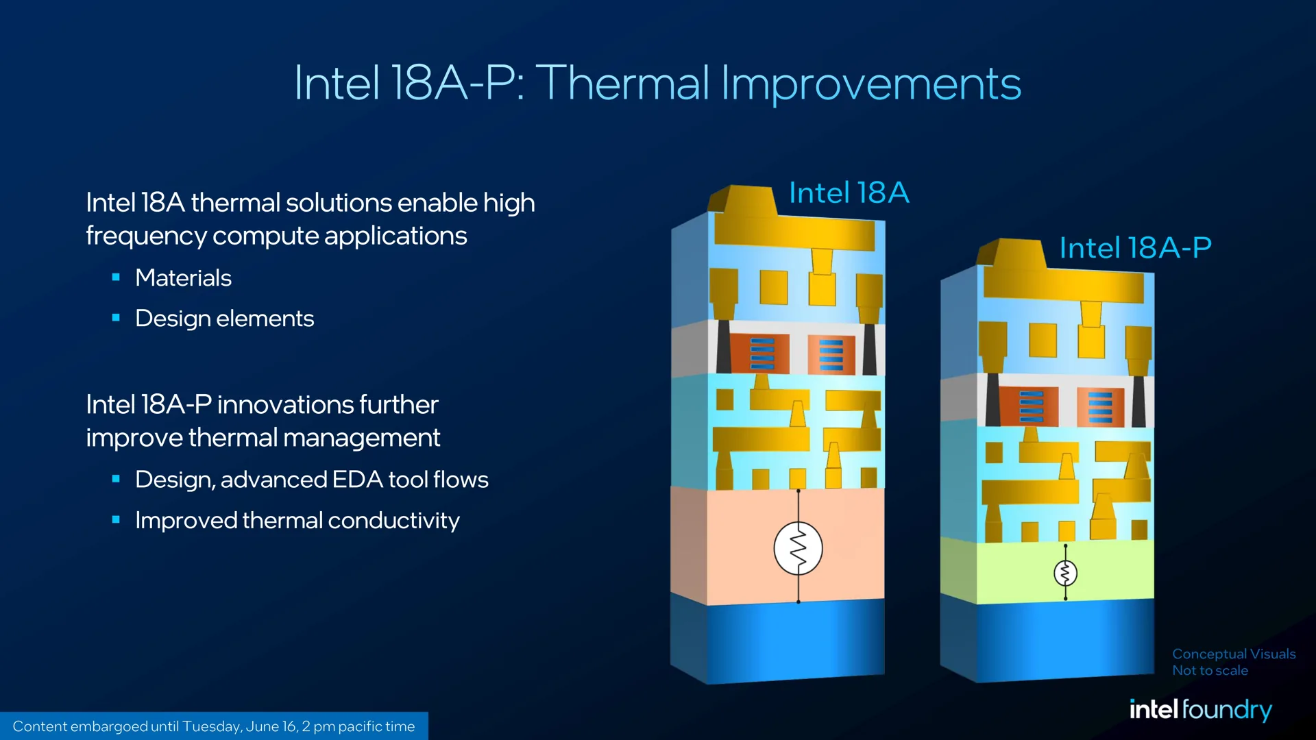
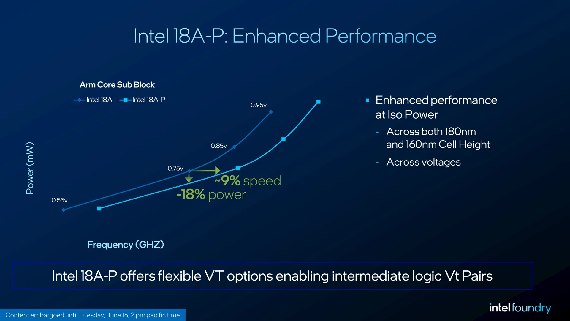
Intel 18A P is the first performance focused extension of the Intel 18A family and entered risk production in June 2026. Intel says the node maintains design rule compatibility with Intel 18A while introducing optimized RibbonFET transistor configurations and additional threshold voltage options. The company currently claims up to a 9% improvement in performance per watt compared with the original Intel 18A process.
That compatibility could allow customers with existing Intel 18A designs to move toward 18A P without completely rebuilding their products. Intel is positioning the enhanced node for demanding artificial intelligence, data center, and high performance computing designs where additional frequency or power efficiency can justify the transition.
The progress follows the Intel 18A P risk production milestone, which showed Intel moving the enhanced process from roadmap presentation toward early manufacturing validation.
Intel 14A represents the more significant long term opportunity. The process introduces RibbonFET 2 transistors and PowerDirect, Intel’s second generation backside power delivery technology. Unlike PowerVia, which routes power through the back of the wafer while maintaining front side transistor contacts, PowerDirect is designed to deliver power more directly to the transistor, potentially improving voltage stability and reducing resistance.
Intel currently projects that 14A could provide between 15% and 20% higher performance at the same power, between 25% and 35% lower power at the same performance, and up to 30% greater chip density compared with Intel 18A. These remain Intel estimates and will depend on product architecture, design libraries, operating voltage, and final manufacturing execution.
Cadence and Intel have already been collaborating on Design Technology Co Optimization for 14A. Cadence expanding its Intel 14A partnership, the companies are attempting to develop process rules, design tools, and intellectual property together rather than waiting until the manufacturing technology is complete. This approach can help ensure that the node is practical for real customer products instead of existing only as a strong transistor demonstration.
The latest certification also extends into advanced packaging. Cadence and Intel have developed a reference design flow supporting Intel’s Embedded Multi Die Interconnect Bridge and EMIB T technologies. The workflow allows engineering teams to design multiple chiplets and their package together while conducting early thermal, signal integrity, and power integrity analysis.
This is particularly relevant for artificial intelligence accelerators and high performance processors, where the final product may combine compute dies, input and output chiplets, cache, memory controllers, and High Bandwidth Memory inside a single package. Cadence says its workflow reduces data conversion requirements and allows package and silicon development to progress concurrently.
Cadence and Intel have also completed silicon validation of interface and memory intellectual property through test chips manufactured on Intel 18A. Physical silicon validation offers stronger evidence than software simulation alone because it demonstrates that Cadence intellectual property, design flows, and Intel’s backside power architecture can operate together on manufactured hardware.
However, certification does not mean Intel 14A is ready for immediate volume production. It means Cadence’s tools and reference methodologies have been aligned with the current Intel process design kits, giving customers a foundation for early design and evaluation work. Intel must still demonstrate stable yields, predictable production schedules, competitive costs, and successful external customer products.
The ecosystem challenge is substantial. TSMC has spent years building its Open Innovation Platform, which combines certified EDA tools, silicon proven intellectual property, design services, cloud infrastructure, and advanced packaging support. TSMC describes it as the foundry industry’s earliest and most comprehensive EDA certification program, creating a deeply established environment for customers developing advanced chips.
Cadence certification therefore does not erase TSMC’s ecosystem advantage, but it addresses one of Intel Foundry’s most important weaknesses. Customers considering Intel need confidence that the design experience will be supported by familiar industry tools and that the node will not require an unnecessary level of additional engineering work.
Intel cannot challenge TSMC through transistor performance alone. The company needs an ecosystem capable of supporting customers from the earliest architectural decisions through design, verification, packaging, and volume manufacturing.
Cadence’s certification is important because it moves Intel 18A P and 14A closer to that complete foundry model. Engineers can use established tools rather than adopting an isolated workflow created specifically for Intel, while silicon validated intellectual property and EMIB support reduce some of the technical risk surrounding future chiplet products.
The larger test remains external execution. Intel 18A P must convert risk production into dependable customer supply, while 14A needs major designs that prove RibbonFET 2 and PowerDirect can deliver competitive performance, efficiency, yields, and costs.
TSMC still holds the stronger manufacturing record and the more mature design ecosystem. However, every validated tool, intellectual property block, and packaging flow makes Intel a more credible alternative for companies seeking advanced capacity and supply chain diversification.
Can a stronger Cadence ecosystem help Intel Foundry compete with TSMC, or will manufacturing yields remain the decisive factor?
