
SK hynix Reportedly Targets 2.5D Advanced Packaging Production In The United States, Eyeing Indiana As A New HBM Scale Lever
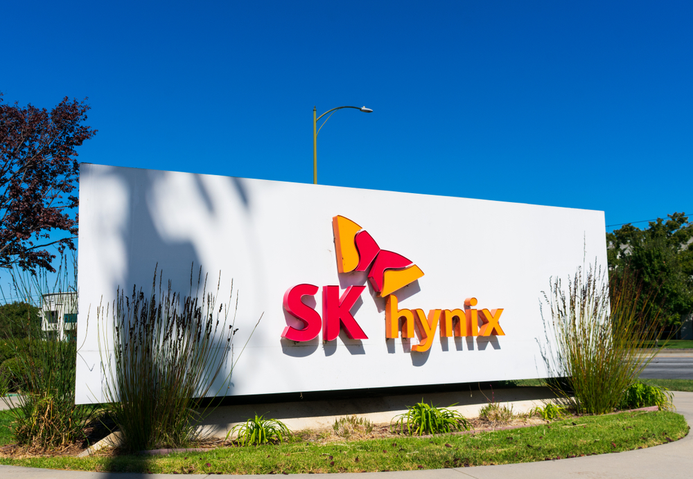
SK hynix is reportedly preparing a major strategic pivot that could reshape how high bandwidth memory reaches next generation accelerators in the United States. According to a local report, the company is discussing plans to establish its first 2.5D packaging mass production line at its new packaging site in Indiana, specifically in the Lafayette area, in a move designed to strengthen its end to end capability beyond memory fabrication and into the critical integration step that increasingly dictates AI system throughput, thermals, and delivery schedules.
The rationale is simple but high impact. HBM demand is surging, and 2.5D packaging is the connective tissue that makes modern accelerators viable at scale by enabling HBM stacks and a processor to be integrated via a silicon interposer. In other words, even if the memory supply is healthy, constrained packaging capacity can still throttle final shipment volumes, creating a bottleneck that ripples straight into customer allocation and launch timing for major platforms.
The report frames this as a response to today’s structural imbalance in advanced packaging availability, where 2.5D packaging for AI accelerators has effectively been dominated by TSMC, while mainstream domestic 2.5D capacity inside the United States remains limited. For SK hynix, that means relying on external 2.5D capacity can introduce both supply constraints and schedule exposure at the exact moment customers are demanding tighter predictability, higher volume, and faster iteration cycles.
Importantly, this is not positioned as a solo build. The same reporting indicates SK hynix is actively discussing the plan with packaging partners, acknowledging that operating advanced packaging lines at the scale needed for large system in package footprints is a different competency stack than memory manufacturing alone. If executed, the payoff is strategic leverage: SK hynix could eventually move toward a turnkey model where it offers both HBM and the associated 2.5D packaging path under a more controlled execution framework, reducing multi party friction when qualification issues appear late in the pipeline.
On timeline and investment, the Indiana packaging site is described as SK hynix’s first United States factory, targeting operations in the second half of 2028, backed by an announced investment of {United States 3.87 billion dollars: 3.87 billion$}. The report also notes that while the company is evaluating multiple utilization options for the Indiana facility, no final decision has been confirmed yet, which signals this is still in a planning and alignment phase rather than a locked deployment schedule.
For the gaming and enthusiast ecosystem, this is worth tracking even if the immediate driver is AI. Advanced packaging capacity increasingly influences how quickly flagship silicon platforms scale, and any step that reduces integration bottlenecks can ultimately improve supply stability across the broader compute stack, including the accelerators and infrastructure that influence everything from cloud gaming performance to content creation workflows.
Do you think memory leaders like SK hynix building 2.5D packaging capacity in the United States becomes a new industry standard, or will most companies continue to lean on foundry led advanced packaging for the foreseeable future?