
Samsung Reportedly Pivots Taylor Texas Fab From 4nm To 2nm GAA, Raising Initial Output Targets To Challenge TSMC
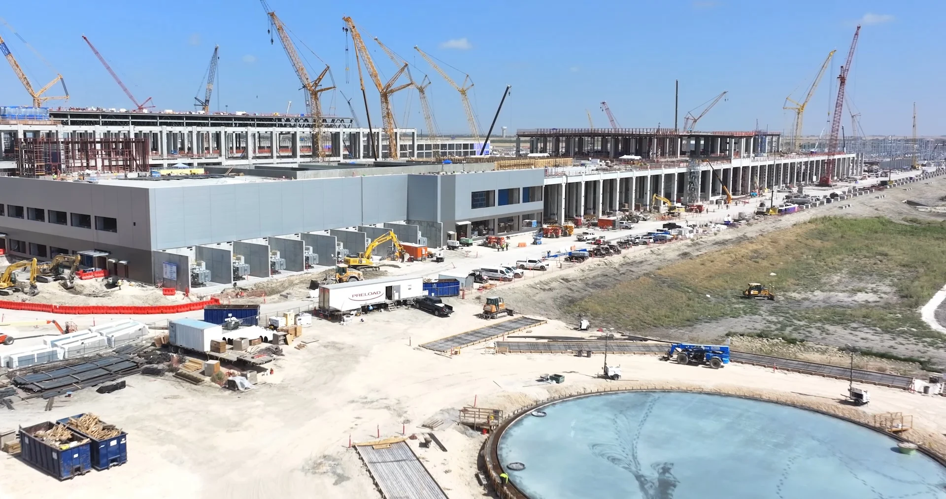
Samsung is reportedly recalibrating its United States foundry roadmap in a way that could materially shift the competitive landscape for advanced logic manufacturing on American soil. Instead of prioritizing a 4 nm ramp at its Taylor, Texas facility, the company is now said to be aligning the site around 2 nm gate all around technology, positioning the plant as a front line node rather than a transitional stop on the process ladder.
The strategic context here is straightforward. TSMC has been widely perceived as cautious about deploying its most cutting edge nodes outside Taiwan at the earliest stages, and that creates a window for Samsung Foundry to differentiate through speed of execution and regional availability. Samsung’s move, if it holds, is an attempt to convert that window into long term account control by offering customers a credible 2 nm manufacturing footprint in the United States.
Operationally, the discussion is not just about a node label. Advanced nodes rely on extreme ultraviolet lithography and a tightly integrated production ecosystem to deliver yield stability, cycle time predictability, and commercially viable wafer economics. Reports referencing earlier equipment activity at Taylor have framed EUV readiness as a key prerequisite to moving below the 5 nm class at scale, which is why any change in equipment purchase plans to support 2 nm is a consequential signal rather than a minor adjustment.
One of the most notable claimed deltas is capacity planning. The initial mass production goal is described as rising from 20,000 wafers per month to 50,000 wafers per month, with longer range expectations that Taylor could reach 100,000 wafers per month by 2027 if ramp, tooling, and demand all align. That would put Samsung in the conversation for meaningful United States volume at the same time the broader ecosystem is pushing for more domestic supply resilience.
On the product and customer pull through side, Samsung has already pointed to Exynos 2600 as its first 2 nm GAA chipset, and early yield chatter has floated around 50 percent, with expectations that yields can improve as process learning compounds. The bigger business development headline tied into this narrative is Samsung’s reported {United States 16.5 billion dollars: 16.5 billion$} Tesla agreement to manufacture the AI6 autonomous driving chip, which would provide a high visibility volume anchor and a high pressure execution benchmark for the foundry organization.
There is also reporting that Samsung has secured 2 nm related demand from Chinese cryptocurrency equipment makers, although commentary suggests that production localization decisions may keep some of that output in Korea rather than routing it through the United States site. If true, that would imply Samsung is segmenting workloads by geopolitics, customer requirements, and internal capacity risk management, rather than treating Taylor as a one size fits all destination.
A forward looking plan only becomes a competitive weapon when it clears execution gates. The core metrics to watch are yield stability over time, tool install and qualification cadence, customer tape out and risk production timing, and whether Samsung can sustain a predictable ramp without the kinds of setbacks that have historically challenged leading edge transitions. In other words, the headline is the roadmap, but the differentiator is repeatable manufacturing performance.
If Samsung can deliver stable 2 nm volume in Texas first, do you see developers and hardware brands shifting more flagship silicon away from TSMC, or will ecosystem inertia keep most of the high end pipeline locked in place?