
Intel EMIB Draws Fresh Attention as Analyst Cites 90% Yield and Intel Maps EMIB T Beyond 12x Reticle by 2028
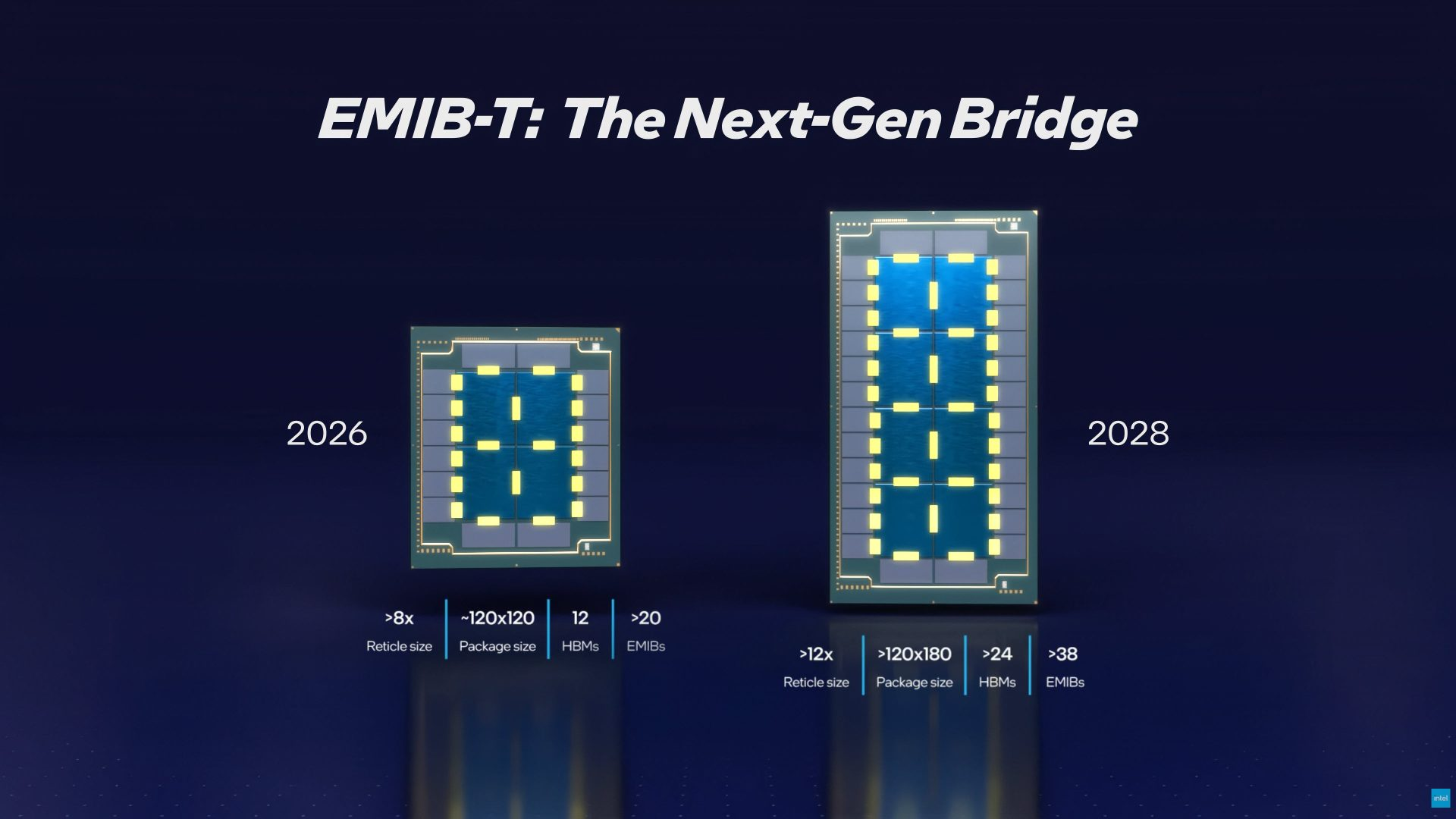
Intel’s EMIB packaging technology is back in focus after analyst Jeff Pu said in a post on X that EMIB has reached 90% yield, a figure that, if accurate in production relevant terms, would mark a meaningful confidence boost for Intel Foundry’s advanced packaging push. The timing matters because Intel’s own foundry roadmap is already pointing to EMIB T scaling beyond 8x reticle in 2026 and beyond 12x reticle by 2028, putting the technology at the center of Intel’s pitch for very large AI and high performance compute packages.
Abstract of MediaTek (2454 TT) Earnings Note & Implications
— Jeff Pu (@sssjeffpu) April 30, 2026
Following our report on March 25 (On Path to >NT$200 EPS) and April 27 (Two More Things!), MTK’s share price has risen by ~50%, and we expect it to react positively post today’s earnings. We raised TP to NT$3,528…
What makes EMIB strategically important is not just the headline number, but the economics Intel is attaching to the platform. In Intel’s recent foundry packaging material, the company says EMIB T can deliver around 90% wafer utilization for bridge dies, versus levels that can fall as low as 60% for large interposer based approaches once packages move beyond 8x reticle class designs. That is the kind of efficiency argument Intel needs if it wants EMIB to be seen as a serious packaging option for large scale AI silicon rather than just an internal technology showcase. Intel also frames EMIB as a way to push beyond reticle limits without the cost and complexity of full size stitched interposers.
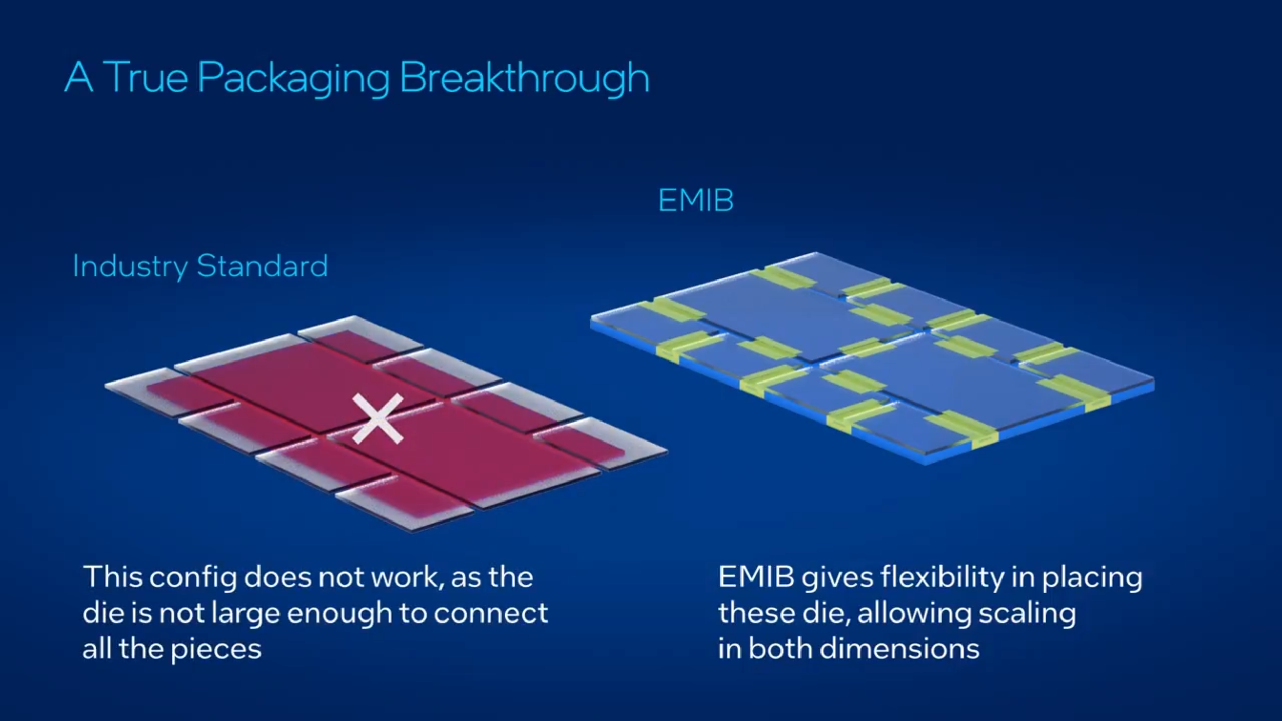
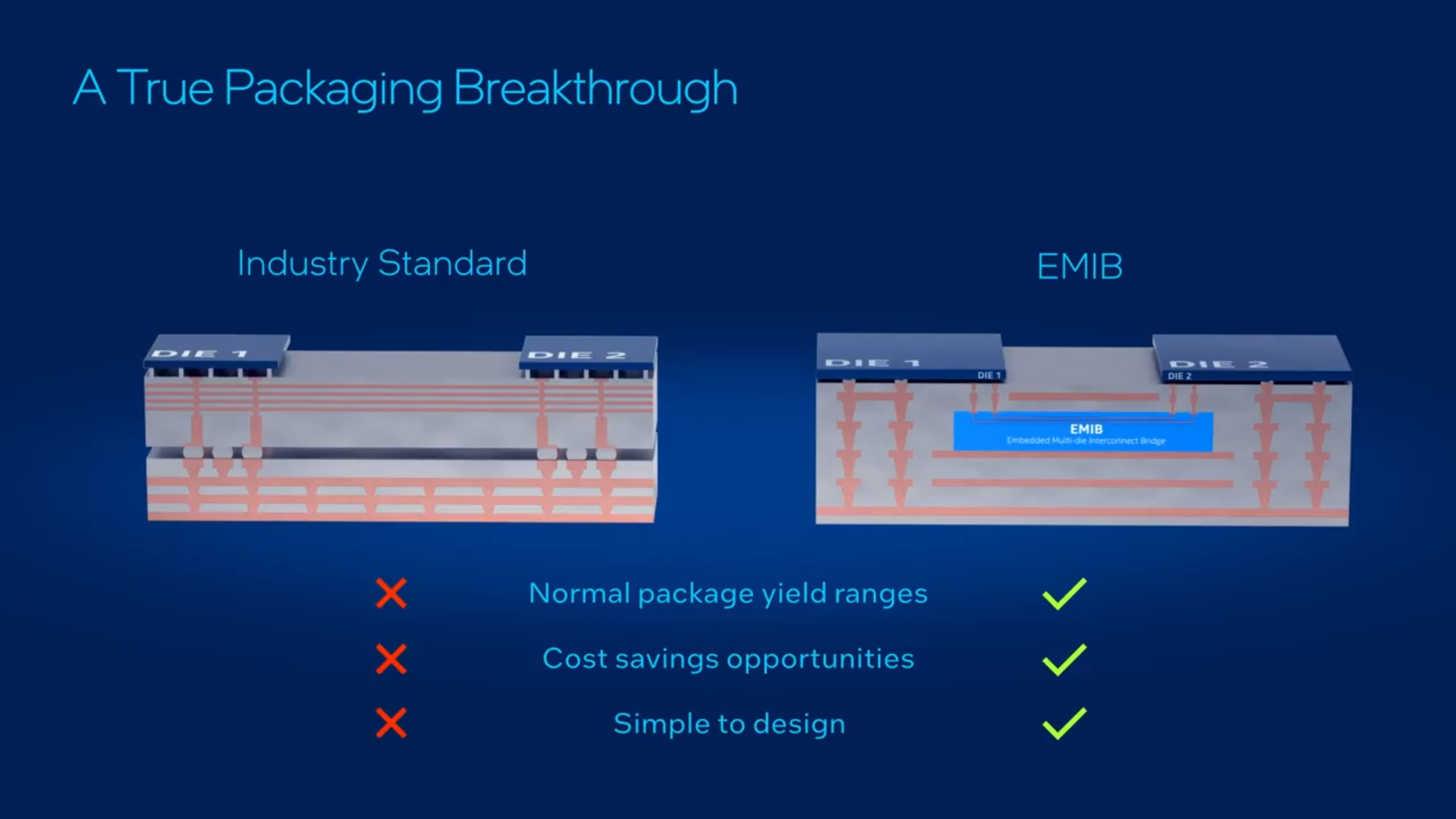
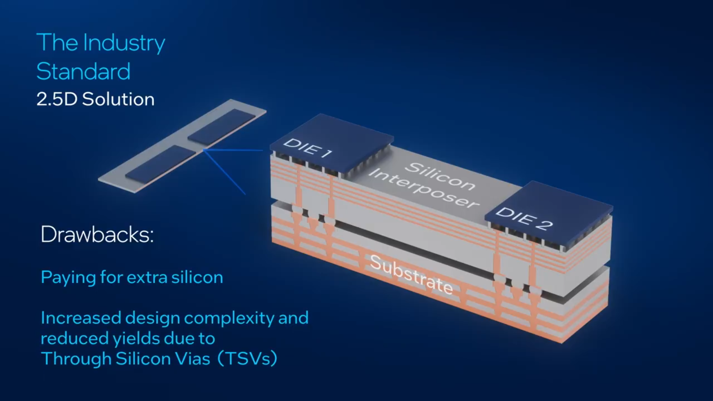
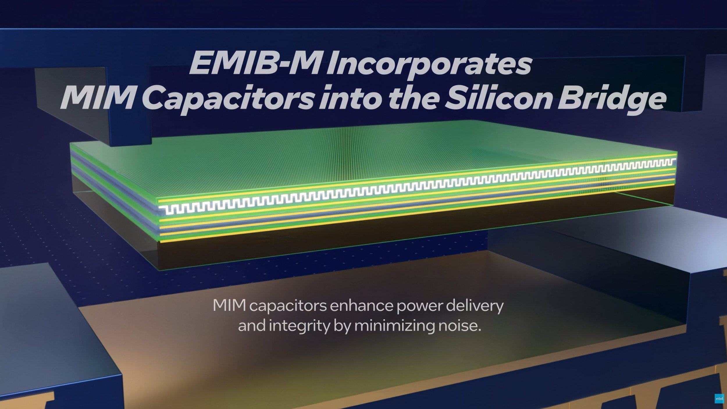
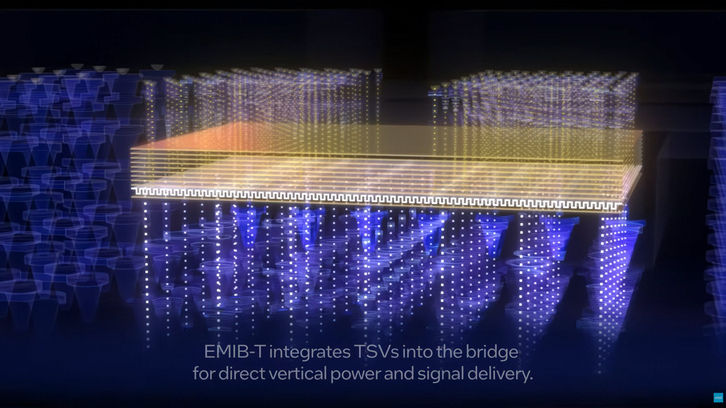
From a technical standpoint, Intel is now clearly separating the EMIB family into 2 tracks. EMIB M is aimed at efficiency and power integrity, using MIM capacitors in the bridge, while EMIB T adds TSVs to improve power delivery and support much larger, denser packages. Intel’s packaging page positions EMIB as production proven since 2017 with both Intel and external silicon, while a new Intel EMIB video continues to reinforce the company’s pitch around lower cost, lower power, higher yield potential, and practical mixed node integration.
The long range scaling story is where Intel appears most eager to make noise. Intel’s official foundry blog says EMIB T enables systems exceeding 6x reticle size today, scales beyond 8x this year, and targets more than 12x by 2028. In the same roadmap discussion, Intel says that 2028 class EMIB T designs are meant to accommodate 16 or more HBM4 or HBM5 stacks using 30 or more EMIB T bridges, giving a clear signal that the company is thinking well beyond mainstream chiplet packaging and directly at the hyperscale AI era.
That means the real takeaway here is less about one analyst post and more about alignment. The analyst signal, Intel’s own utilization claims, and the official scale roadmap are all pointing in the same direction. Intel wants EMIB T to be viewed as one of the company’s core advanced packaging differentiators, especially for customers that need very large heterogeneous packages without absorbing the full penalty of giant interposer designs. Whether that becomes a genuine foundry breakthrough will still depend on customer wins and sustained manufacturing execution, but the roadmap now looks much more concrete than it did a year ago.
Do you think EMIB T has what it takes to become a real large package contender for next wave AI chips, or does Intel still need stronger proof through customer products first?