
NAURA Demonstrates 64 Layer 3D DRAM Etch Process as China Pushes Beyond EUV Limits
Chinese semiconductor equipment manufacturer NAURA Technology Group has demonstrated a cyclic etching process for 3D DRAM structures, achieving highly selective processing across 64 alternating silicon and silicon germanium layers. The development could become important for China's memory industry as manufacturers explore new device architectures to extend DRAM scaling.
The technology was detailed in a CSTIC 2026 research paper titled "Cyclic Etching of SiGe/Si Multilayers with Fluorine Chemistry for 3D DRAM Applications." Presented at the China Semiconductor Technology International Conference in March 2026, the work remains a research demonstration rather than a commercially qualified manufacturing process.
3D DRAM is not simply DRAM stacked in the same way as 3D NAND. NAND increased density by moving memory cells into tall vertical strings, while future 3D DRAM concepts are exploring ways to restructure DRAM transistors, capacitors, and supporting layers vertically as conventional planar scaling becomes more difficult. The goal is similar in one respect, increasing density through the third dimension, but the device structures and manufacturing requirements are substantially different.
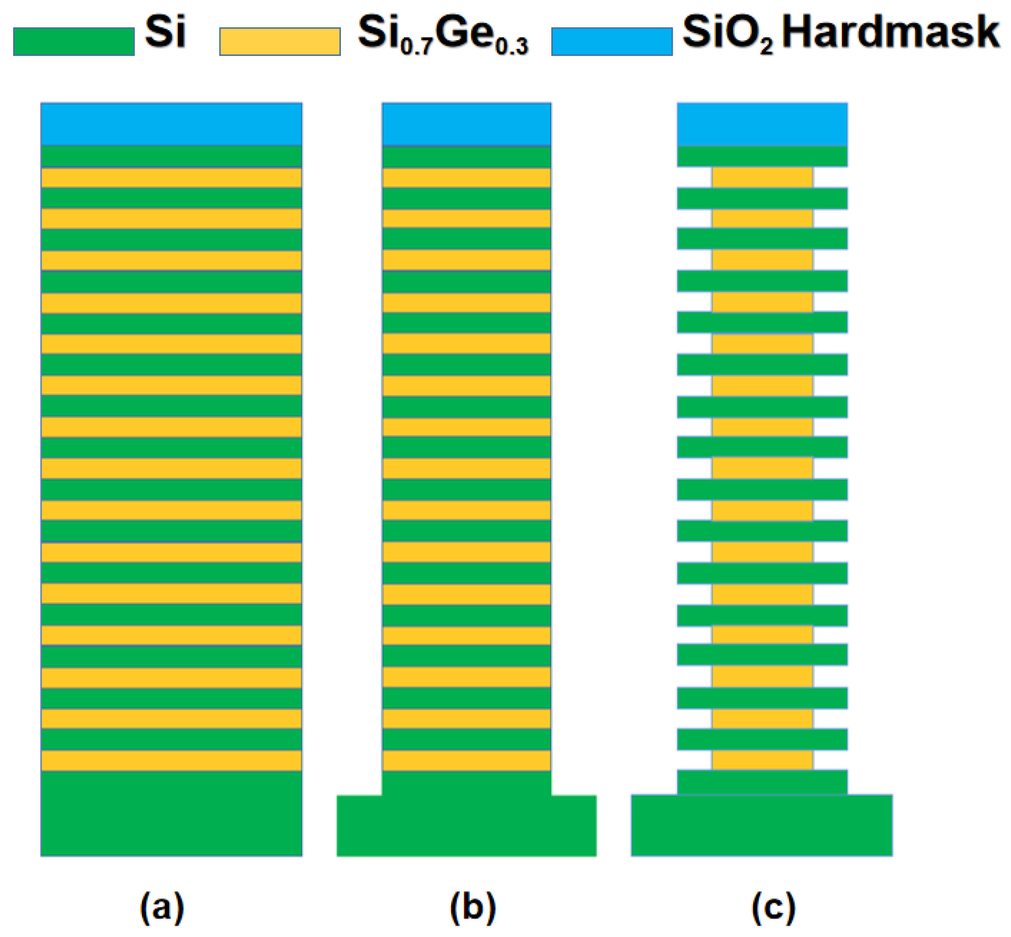
NAURA's process addresses one of those manufacturing challenges. The experimental structure uses alternating silicon and silicon germanium layers, with the silicon germanium selectively removed while preserving the surrounding silicon. Maintaining consistent results becomes increasingly difficult as structures grow deeper because reaction byproducts can accumulate and reduce etching uniformity.
The process uses 2 stages. Fluorine based chemical etching first removes silicon germanium without electrical bias, limiting damage to silicon. A plasma assisted purge then clears reaction byproducts before another cycle begins. NAURA reported silicon germanium to silicon selectivity above 500:1, meaning the targeted material was removed at more than 500 times the rate of silicon.
The company also reported silicon loss below 10 Å during a 200 nm lateral silicon germanium etch and structural uniformity above 95% across the 64 layer structure. Those results are notable because future 3D DRAM manufacturing will require highly controlled etching throughout increasingly complex vertical structures.
The development is particularly relevant to China's semiconductor industry because access to the most advanced EUV lithography equipment remains restricted. While leading global memory manufacturers continue using advanced lithography alongside new materials and device structures to extend DRAM scaling, Chinese suppliers have additional incentives to invest in DUV optimization, domestic semiconductor equipment, advanced etching, deposition, and alternative architectures.
This does not mean 3D DRAM eliminates the need for advanced lithography. Even vertically structured memory still requires demanding patterning, deposition, alignment, etching, and process control. However, shifting more of the scaling challenge into the vertical dimension could reduce the extent to which density improvements depend exclusively on shrinking every feature horizontally.
NAURA's research therefore matters primarily as an equipment and process milestone. If its cyclic etching method can eventually meet commercial requirements for throughput, yield, defect control, reliability, and cost, it could contribute to a broader domestic manufacturing ecosystem for next generation memory.
China's largest DRAM producer, CXMT, is also pursuing more advanced memory technologies, including HBM and new transistor architectures. Its recent technology developments illustrate the broader pressure on Chinese memory manufacturers to find new scaling methods. However, there is currently no public evidence connecting CXMT directly to NAURA's 64 layer etching research or confirming that this specific process is being evaluated for CXMT production.
NAURA's 64 layer result is an important engineering milestone, but it should not be interpreted as China having solved 3D DRAM manufacturing or bypassed EUV restrictions. A successful research demonstration still needs to prove that the process can operate with acceptable throughput, yield, defect density, reliability, and cost in high volume production.
The larger significance is the changing balance of semiconductor scaling. As memory architectures become more three dimensional, deposition, selective etching, materials engineering, and vertical device integration become increasingly important alongside lithography.
That gives domestic equipment suppliers such as NAURA more areas in which to build strategically important technology. The 500:1 selectivity result is therefore best viewed as progress in one critical manufacturing step for future 3D DRAM rather than evidence of a complete production solution.
Could advances in etching and vertical memory architectures reduce the semiconductor industry's dependence on increasingly aggressive horizontal DRAM scaling?
