
Intel Solves Encapsulation Barrier for AI Packages Beyond 7x Reticle Size
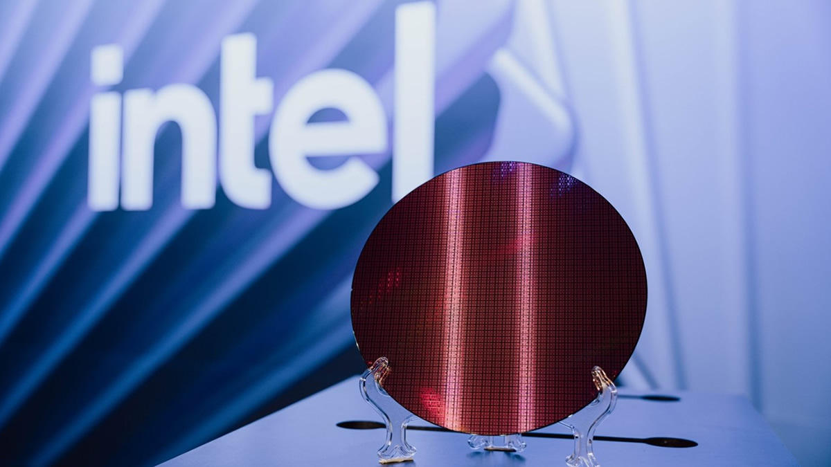
Intel Foundry has developed a void free encapsulation process for advanced semiconductor packages exceeding 7x reticle size, removing one of the major manufacturing barriers facing future artificial intelligence and high performance computing processors. The research supports Intel’s wider plan to create Hyper Large Form Factor packages measuring as much as 240 mm by 240 mm, allowing significantly more compute dies, High Bandwidth Memory stacks, and connectivity components to operate within a single system.
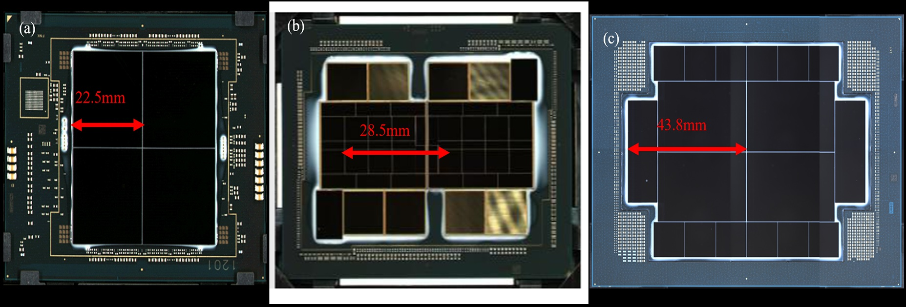
Advanced packages depend on underfill material flowing underneath each chip and sealing the electrical joints connecting it to the substrate. This protective layer reduces mechanical stress, prevents contamination, and improves long term reliability. Earlier package designs required underfill to travel approximately 22 mm, while current large EMIB packages can exceed 43 mm. Larger chip assemblies increase the distance further, making it more difficult to achieve complete coverage without trapping air pockets or producing structural defects.
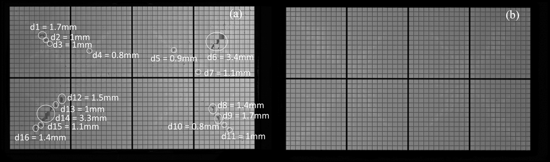
Intel addressed the problem through 3 coordinated changes covering the underfill material, dispensing method, and curing process. The company reduced material viscosity to improve flow while maintaining sufficient mechanical reliability. Engineers also replaced a traditional edge based application with multiple dispensing points positioned around and between dies, reducing the distance the material must travel. Finally, Intel optimized the curing process to collapse remaining air pockets, eliminating defects measuring as much as 3.4 mm during earlier testing.
The process was validated on an EMIB package exceeding 5x reticle size containing 18 dies, including positions for 12 HBM stacks. Intel achieved void free encapsulation across flow distances greater than 40 mm. A larger tiled EMIB design beyond 7x reticle size also produced void free results. Foveros 3D packages at 2x and 4x reticle size achieved the same result, while the 2x design completed 700 temperature cycles and more than 1,000 hours of high temperature reliability testing.
"We’ve moved past the era of one big chip to a system of chips, almost like a silicon mosaic."
— Quote by: Intel Foundry
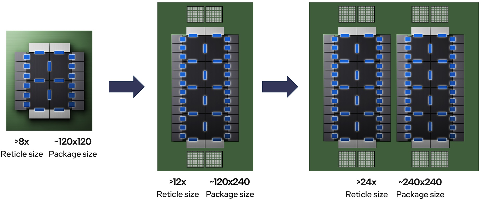
The encapsulation breakthrough supports a much larger architectural blueprint for future AI systems. Intel is researching packages measuring up to 240 mm by 240 mm, with a roadmap extending beyond 12x reticle integration and eventually toward panel scale platforms approaching 50x reticle size. These designs could combine arrays of compute chiplets, HBM stacks, input and output components, and specialized accelerators within one package instead of distributing them across multiple conventional processors. However, Intel has only validated encapsulation beyond 7x reticle size, meaning the full 240 mm platform remains a future engineering objective rather than a production ready product.
Intel’s proposed architecture uses EMIB T bridges with metal layers finer than 2 micrometers and data transfer rates above 64 Gbps per channel. The company is also evaluating copper cable connections and co packaged optics for external communication speeds reaching 448 Gbps. Spare communication lanes could improve bundle yield from approximately 97% to above 99%, which becomes increasingly important as the number of chiplets and interconnects expands.
Power delivery, heat, and structural deformation remain significant challenges. Intel estimates that Hyper Large Form Factor packages could consume between 15 kW and 25 kW while producing localized thermal hot spots. The company proposes embedded silicon capacitors, integrated voltage regulation, modular cooling zones, glass core substrates, and reinforced package structures. Simulations showed that an unsupported package could deform by as much as 7 mm at room temperature, requiring stiffener rings and cooling hardware applying more than 4,500 newtons of pressure to maintain sufficient flatness.
Glass substrates could become particularly important because they offer stronger dimensional stability and lower thermal expansion than traditional organic materials. Intel recently expanded its work with Lens Technology on glass processing, while glass substrate commercialization could begin within approximately 3 years if manufacturing and reliability development remain on schedule.
Intel is positioning advanced packaging as one of its strongest opportunities to attract external foundry customers. EMIB T can connect chiplets without requiring a full silicon interposer, potentially reducing cost while supporting large AI processors with many HBM stacks. This capability has already generated speculation around possible future platforms such as NVIDIA Rubin Ultra, although NVIDIA has not confirmed using Intel packaging for that product.
Intel has not yet manufactured a complete 240 mm by 240 mm processor package, but solving void free encapsulation beyond 7x reticle size represents a meaningful step toward making such architectures technically possible. Packaging larger numbers of dies is not only a design challenge. Every increase in package size introduces additional risks involving material flow, warpage, interconnect yield, power distribution, and cooling.
The commercial opportunity could be considerable because future AI processors may become too large and power intensive for conventional packaging methods. Intel does not necessarily need to manufacture every compute die to participate in that market. It could generate foundry revenue by assembling chiplets produced by several manufacturers into one integrated package.
The next milestone will be demonstrating that these methods can operate reliably at higher volumes and larger dimensions without making manufacturing costs or cooling requirements impractical. Intel has removed one important barrier, but reaching 12x, 24x, or panel scale production will require several additional breakthroughs.
Could advanced packaging become Intel Foundry’s strongest advantage in the artificial intelligence market, even if other manufacturers continue producing the individual compute dies?
