
Intel Reportedly Turns to AUO for Micro LED CPO and Advanced Glass Packaging
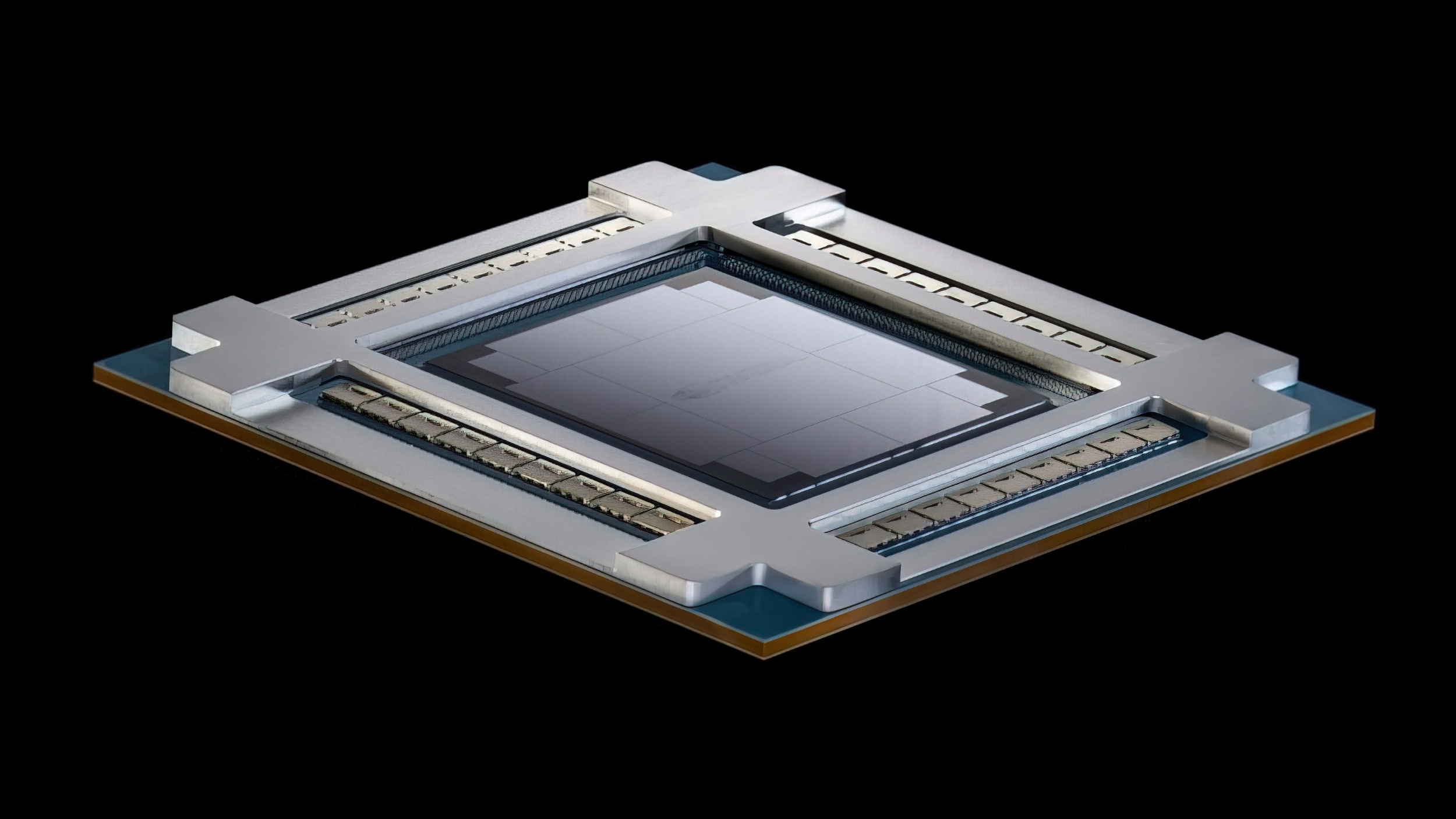
Intel is reportedly working with AU Optronics on advanced packaging technology that could combine AUO’s Micro LED and glass processing expertise with Intel’s growing packaging portfolio. The reported cooperation is focused on co packaged optics, high density compute integration, and glass based packaging for future AI systems, but neither company has formally confirmed the partnership. Intel declined to comment on the report, while AUO has previously acknowledged that it is developing advanced packaging and glass substrate technologies with unnamed partners.
The distinction around Micro LED is important. This is not about placing conventional Micro LED displays inside processors. AUO is developing Micro LED devices as optical transmitters for short distance data communication, using large arrays of small light sources to move information between components. At SEMICON Taiwan 2026, AUO demonstrated a system level Micro LED CPO module targeting links of up to 10 meters inside AI data centers. The design combines Micro LED transmitters from Ennostar, Micro photodetectors from Tyntek, AUO’s mass transfer and optical integration technology, redistribution layer packaging, and Corning fiber solutions.
AUO describes its approach as a wide and slow parallel architecture. Instead of pushing extremely high data rates through a small number of optical channels, large arrays of Micro LEDs collectively carry the traffic. The company says this can reduce dependence on power intensive signal compensation while easing thermal requirements. AUO also lists operation at temperatures up to 125°C and lifetimes exceeding 30,000 hours among the characteristics that make Micro LED attractive for dense AI infrastructure.
The reported Intel connection makes technical sense because both companies are also investing heavily in glass. AUO has nearly 30 years of glass processing experience and is developing through glass vias, redistribution layers, and glass core substrates for advanced semiconductor packaging. Intel has been pursuing the same material as a potential replacement for organic substrates in very large chiplet packages, where better flatness, dimensional stability, and lower signal loss can become increasingly important.
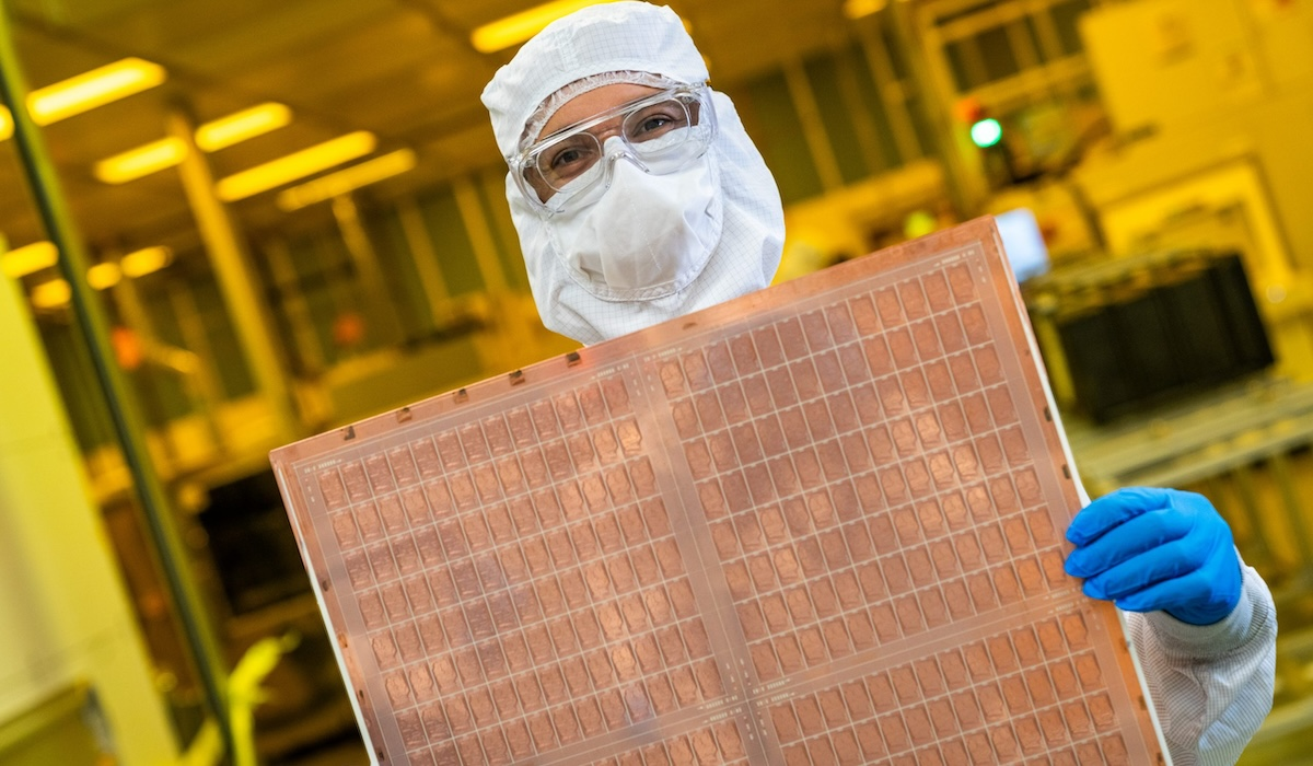
Intel also received a US patent on September 8 for an "IC Package with Micro LEDs." The design places a semiconductor die and Micro LEDs within or around a glass substrate and uses through glass vias to provide electrical connections. However, the patent itself should not be treated as confirmation of the reported AUO partnership or of a finished CPO product. Its documented use cases include visual indicators, lighting effects, and in place electrical testing, while the broader packaging structure overlaps with technologies relevant to heterogeneous optical integration.
The potential partnership would therefore bring together several technologies that are becoming increasingly important as AI systems scale beyond conventional electrical interconnects. Intel contributes EMIB, advanced chiplet integration, and years of glass substrate research, while AUO brings Micro LED manufacturing, optical coupling, redistribution layer packaging, and large scale glass processing. That combination could eventually support packages where compute, memory, and optical communication are integrated much more closely than in current server designs, although there is no announced product or production timeline yet.
The interesting part of this report is not that Intel suddenly wants to become a display company. Micro LED is being repurposed here as a communications technology, and that changes the conversation completely. AUO has spent years mastering the ability to move and integrate enormous numbers of tiny LEDs, while AI infrastructure now needs increasingly dense optical links that consume less power and generate less heat.
Intel already has a serious advanced packaging portfolio, but packaging is becoming a system problem rather than simply a way to connect chiplets. Compute dies, HBM, glass substrates, electrical bridges, and optical links increasingly have to be designed together. If the reported cooperation with AUO develops into a commercial platform, it could give Intel another route into the AI infrastructure supply chain beyond simply manufacturing the compute silicon.
The key point for now is that the cooperation remains reported, not confirmed. AUO has confirmed its Micro LED CPO and glass packaging work, and Intel has confirmed its own glass and advanced packaging development, but neither company has publicly announced a joint product.
Do you think Micro LED based optical links could become a serious alternative to conventional silicon photonics for short distance AI data center connections?
