
Intel Showcases First Glass Core Substrate Integrated with EMIB Packaging
Intel Foundry is signaling that its glass substrate roadmap is still very much alive, using NEPCON Japan as a stage to show what it describes as an industry first implementation that combines a thick core glass substrate with EMIB advanced packaging. The showcase was shared publicly via the NEPCON Japan post, and it positions the technology as a data center focused platform play designed to scale multi chiplet architectures beyond what traditional organic substrate approaches comfortably support.
🟦Intel’s glass core substrate unveiled at NEPCON Japan 2026 can only be described as impressive.
— SemiVision👁️👁️ (@semivision_tw) January 22, 2026
What stands out most is execution. This isn’t about vision alone; assembly and reliability are already underway. It clearly shows how Intel is positioning glass core substrates as a… pic.twitter.com/9JNaCVe9pM
This matters because recent chatter in the market has suggested Intel might have de prioritized glass substrates after internal changes and the departure of key personnel. The NEPCON appearance is effectively a confidence signal to the ecosystem that Intel is still investing in glass as a strategic substrate transition, rather than treating it as a research side quest. Intel has long been viewed as an early mover in glass substrate development, so this public prototype level demonstration is also a credibility reset for anyone who assumed the effort had stalled.
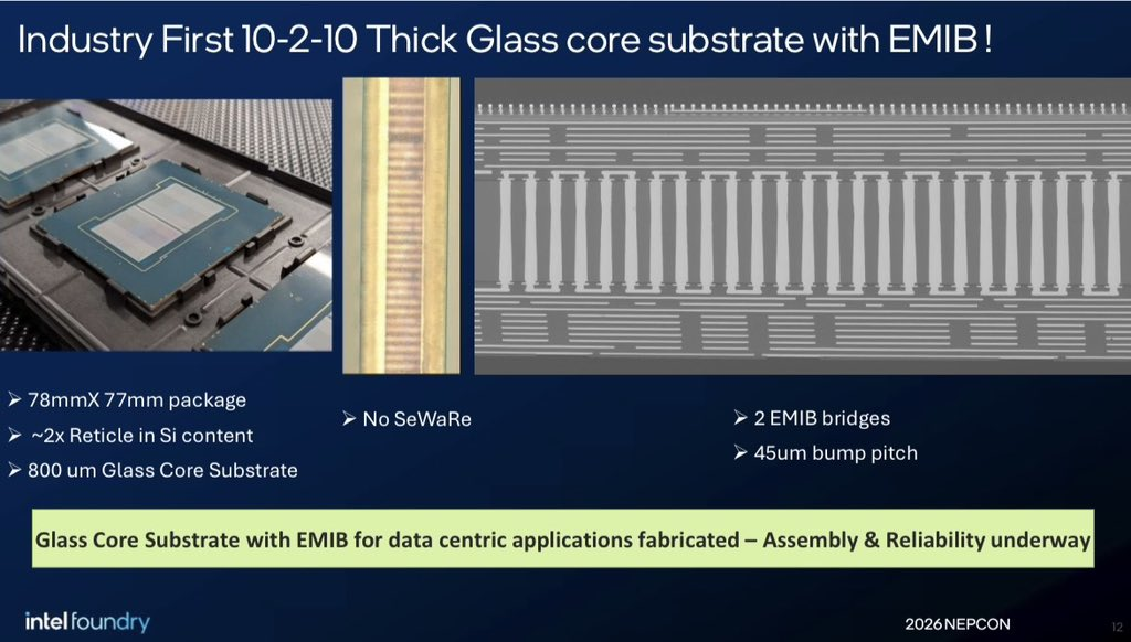
Technically, the details being discussed around the package are the kind that immediately read as future AI accelerator territory. Intel’s approach is said to deliver a 2x reticle sized package at 78 mm x 77 mm, using a dense 10 2 10 stack up structure described as 10 RDL layers, a 2 layer glass core, and 10 bottom build up layers. The implication here is clear: glass is being leveraged to maintain dense wiring capability even at a high layer count, which is exactly the direction the industry needs if it wants to keep scaling bandwidth and interconnect density as chiplet counts climb.
Intel has also reportedly integrated 2 EMIB bridges within the package to connect multiple compute dies, which aligns with the broader industry shift toward modular compute design. In practical terms, EMIB is a bridge based interconnect approach that can help enable large multi die assemblies without forcing every design into a full silicon interposer strategy. That is especially relevant right now because advanced packaging capacity constraints have become a real bottleneck for AI roadmaps, and any solution that offers flexibility in how chiplets are stitched together is going to attract interest from HPC and AI focused silicon teams.
The showcase also appears to highlight a server oriented intent, including markings that indicate a focus on reliability and warpage control, both of which are critical when you are building large footprint packages designed for long duty cycles. The pitch is that glass substrates can support fine connections, better depth of field control, and reduced mechanical stress, which helps make large super packages more viable as designs push toward dozens of chiplets in a single assembly.
The bigger strategic read is that Intel Foundry is trying to turn advanced packaging into a revenue growth lane, not just a supporting capability for internal products. If Intel can keep moving with EMIB plus glass enablement while the supply chain remains constrained, it could create a differentiated capacity and technology offering that attracts external HPC customers looking for alternatives and additional production paths.
If you are building next gen AI silicon, do you see glass substrates as the real unlock for mega chiplet packaging, or do you think the industry will lean harder on other interconnect approaches first?