
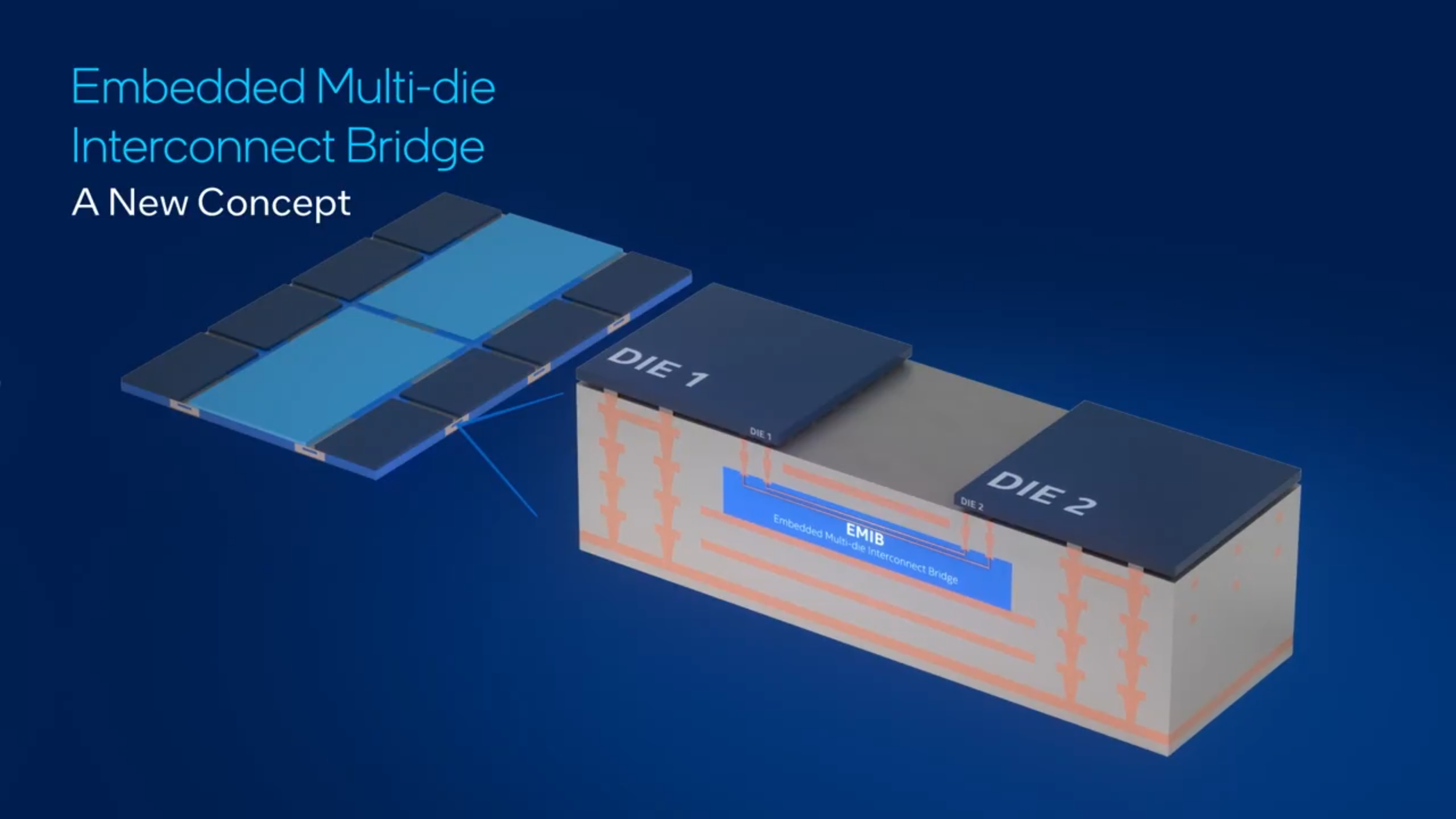
Intel Positions EMIB As A Stronger Alternative To Traditional 2.5D Packaging
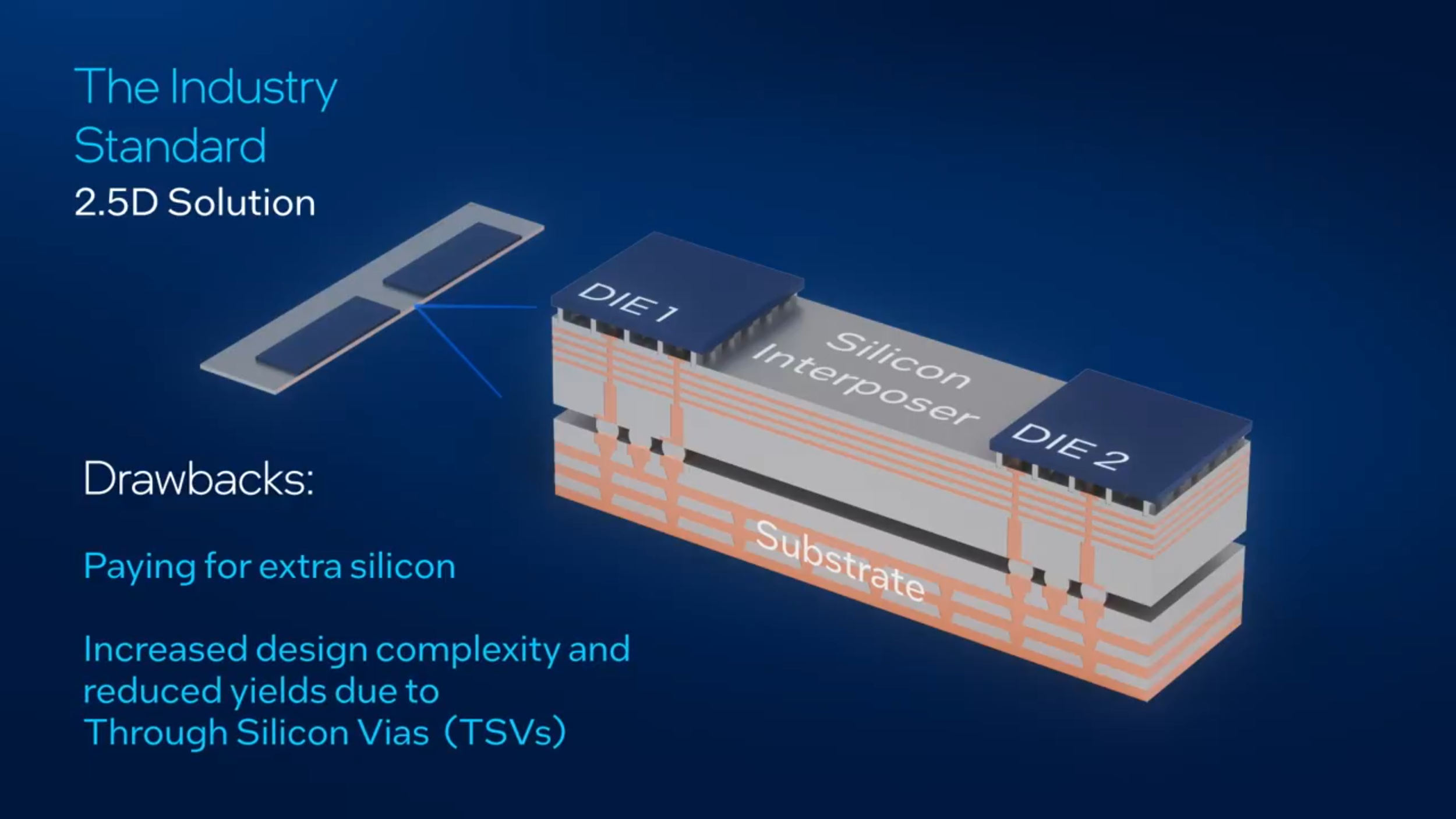
Intel is making a renewed push to differentiate its advanced packaging stack, arguing that its EMIB interconnect approach offers measurable advantages over traditional 2.5D packaging methods that rely on full silicon interposers. In Intel’s framing, the core value proposition is straightforward: instead of paying for large areas of silicon that exist primarily to route connections, EMIB uses small embedded bridges placed only where dies need high density links, aiming to improve cost efficiency, simplify design tradeoffs, and preserve more typical package yield ranges as chiplets scale.
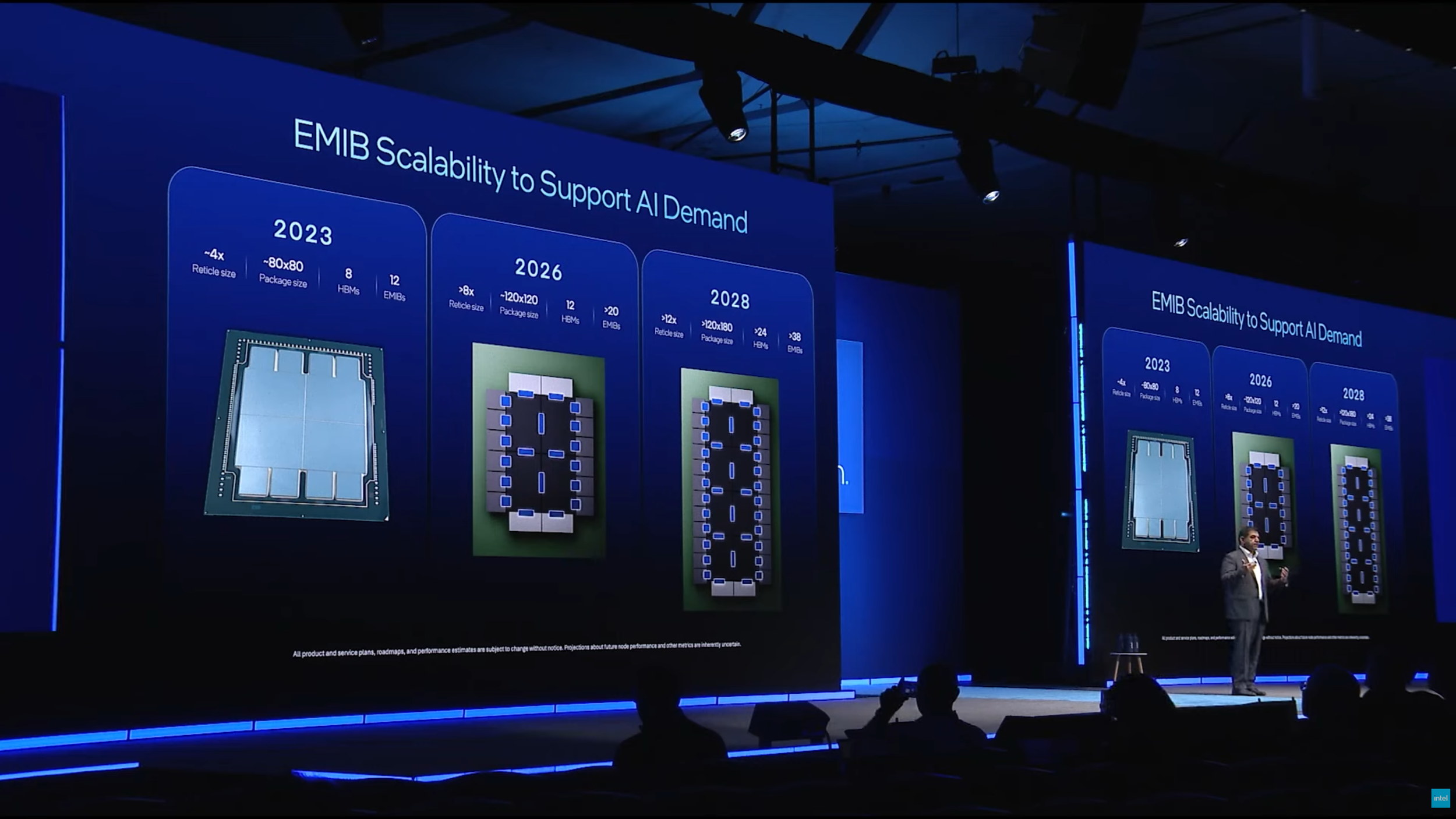
Intel’s messaging matters because the industry is now firmly in a chiplet era. Data center CPUs, AI accelerators, and heterogeneous compute platforms are increasingly built as multi die systems where the interconnect and packaging strategy can be just as decisive as the process node itself. Intel notes that EMIB has already been deployed across multiple high complexity products, including major server and data center platforms, and the company is now positioning EMIB plus its broader packaging portfolio as a key pillar for both internal roadmaps and Intel Foundry customer opportunities.
Built for chiplet flexibility, EMIB supports high-speed die-to-die signaling with simple I/O and per-link bridge customization—so every connection is optimized for performance.
— Intel Foundry (@Intel_Foundry) January 14, 2026
Learn more: https://t.co/aviRs6rJUI#IntelFoundry #Semiconductors pic.twitter.com/OHFg7SP272
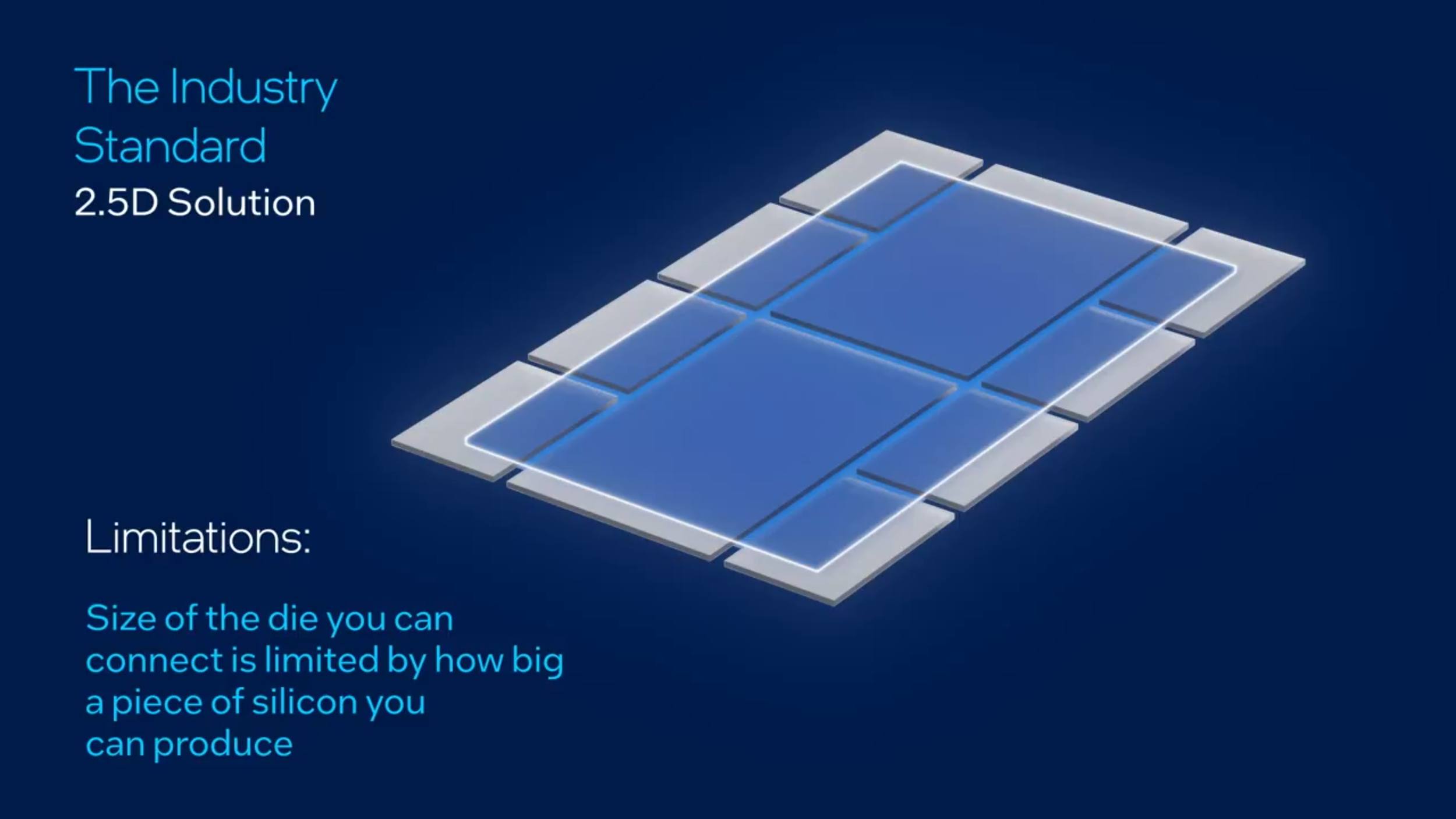
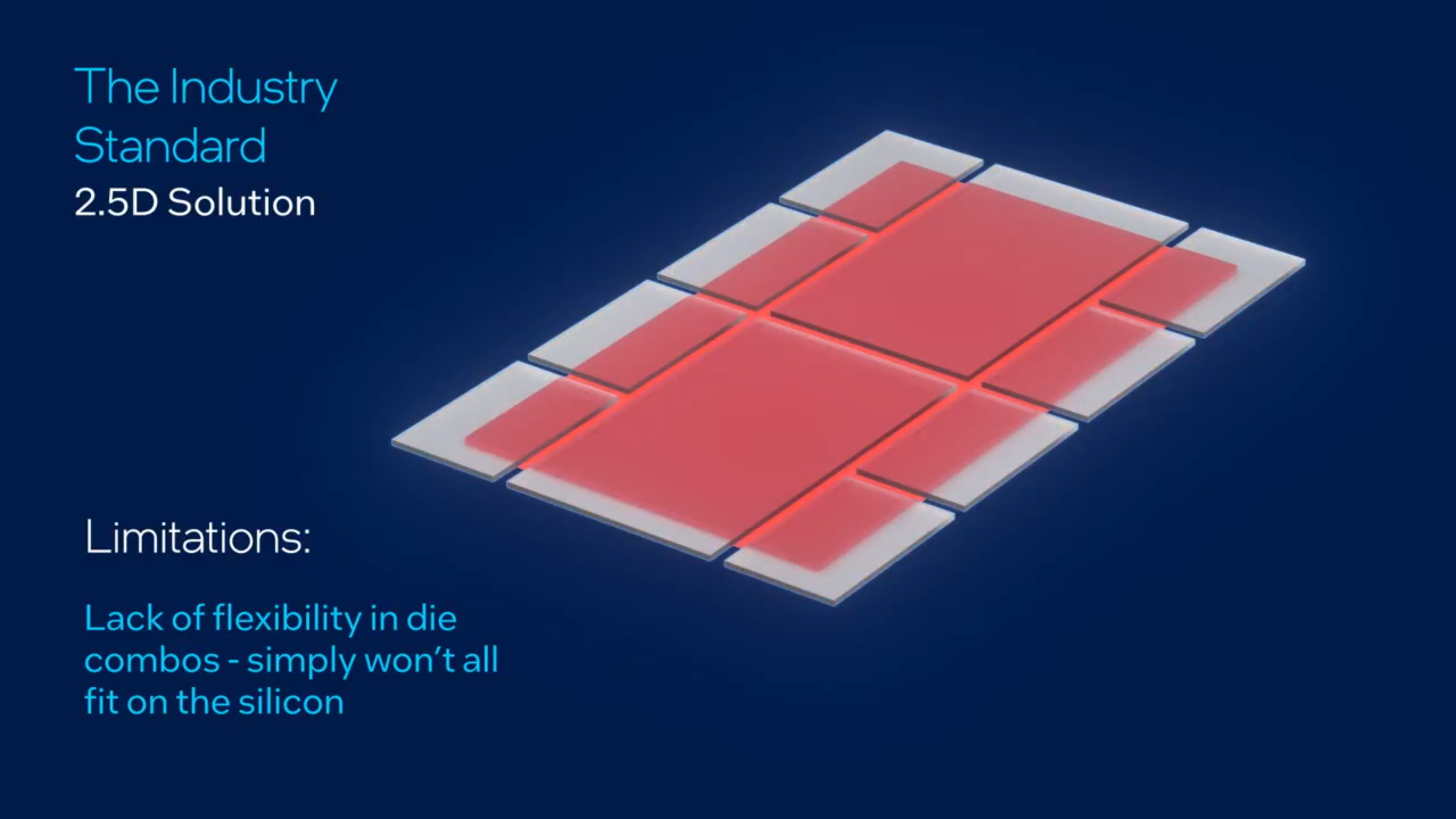
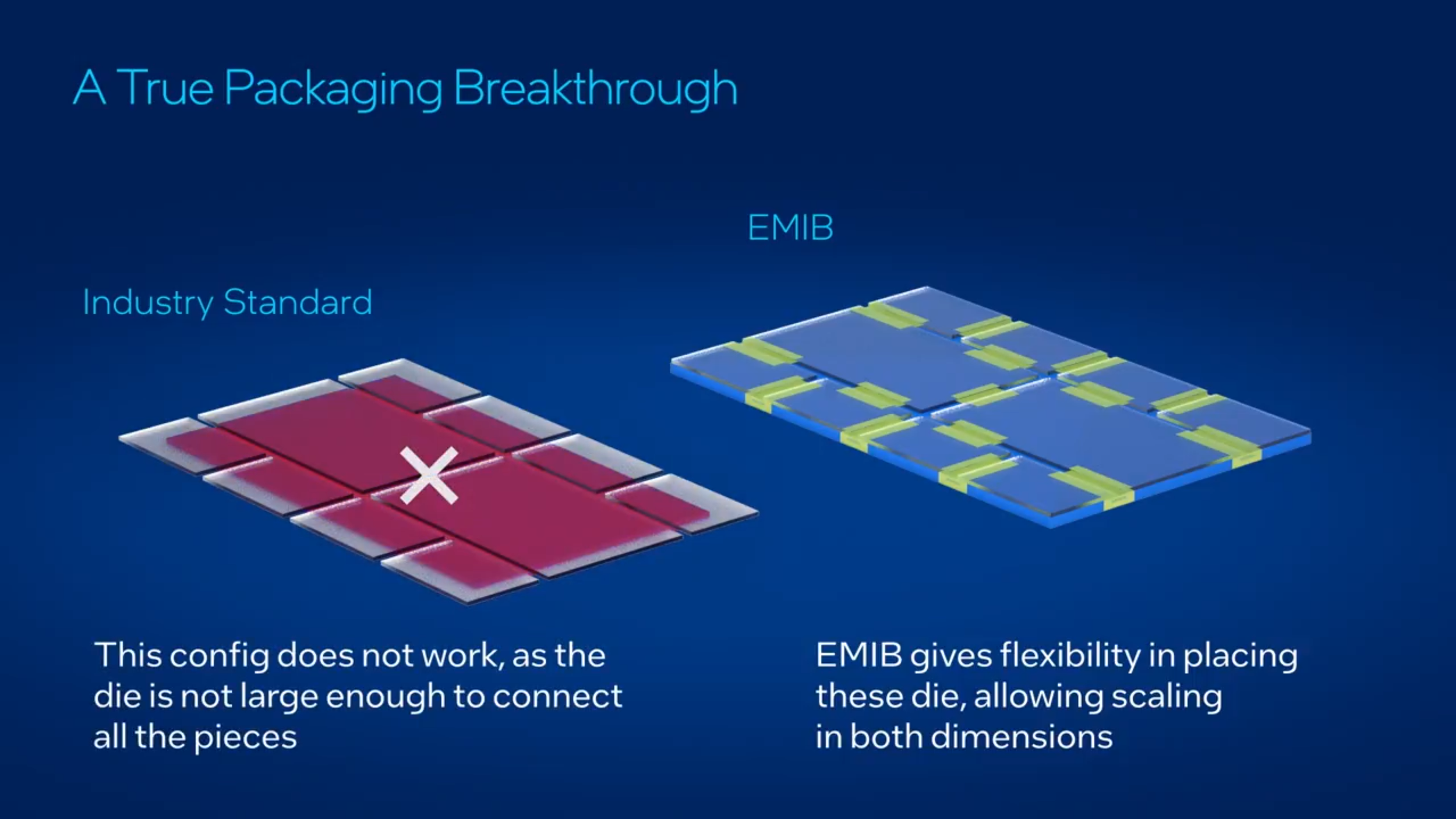
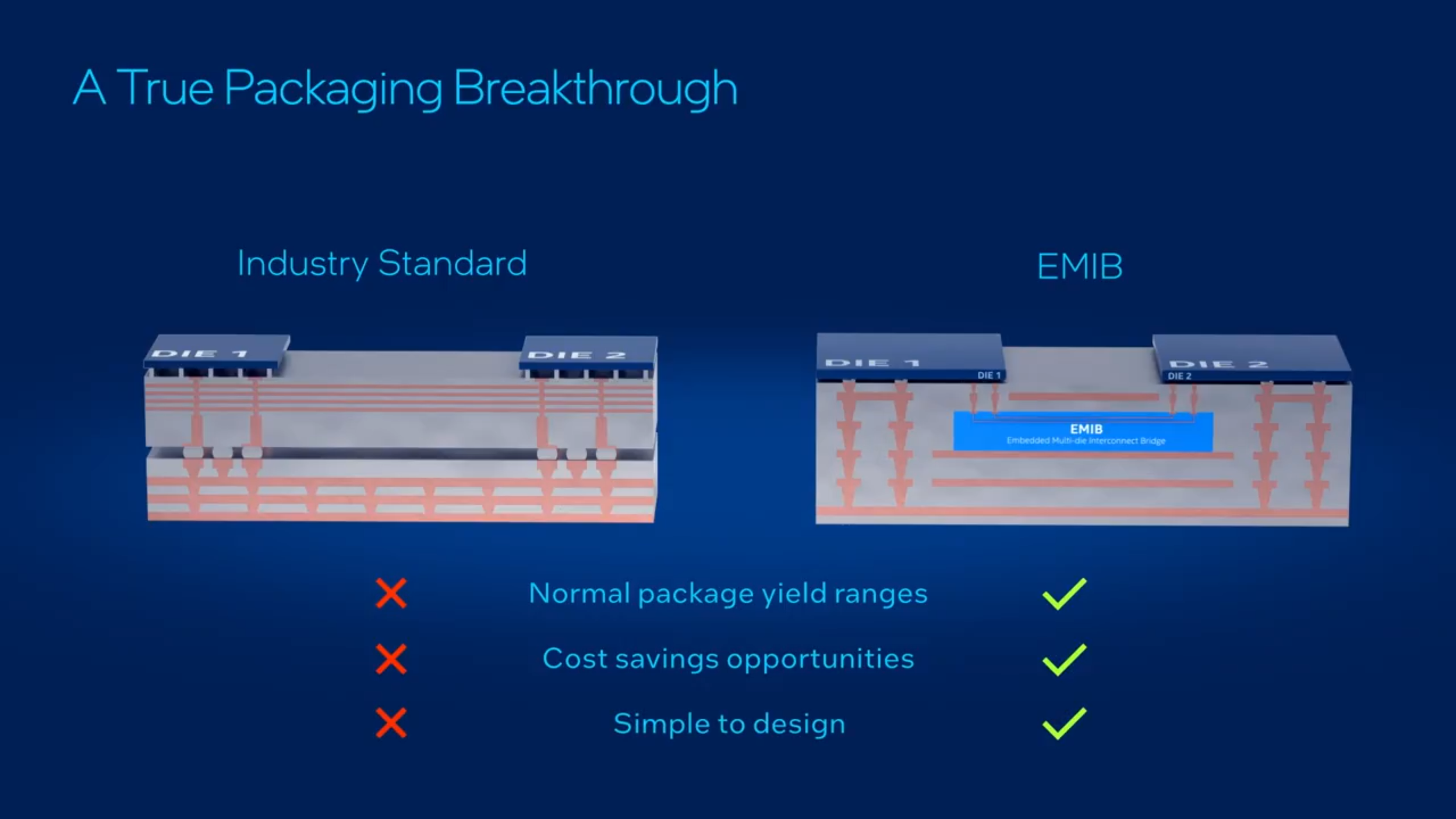
Intel contrasts EMIB against conventional 2.5D packaging where chiplets sit on a silicon interposer. In that classic approach, the interposer is effectively a large piece of silicon used to route signals between dies through dense wiring structures, and as package size increases, design complexity and cost typically rise. Intel argues this creates a double pressure point: you pay for silicon that is not performing compute work, and yields can become more sensitive as complexity and interposer scale increase.
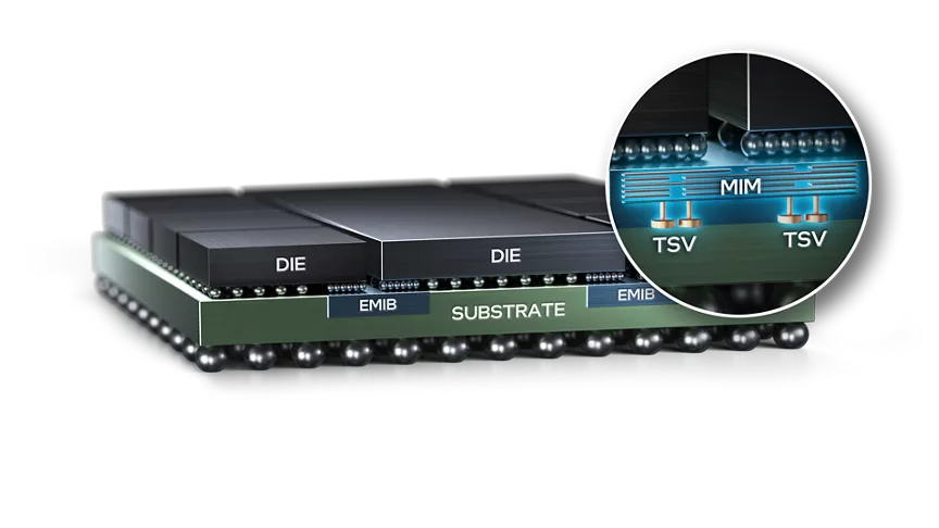
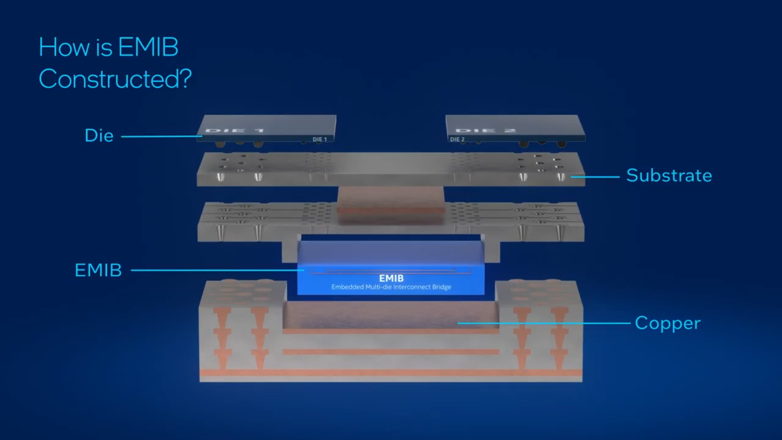
EMIB sidesteps the large interposer by embedding a silicon bridge inside the package substrate. The bridge can be placed only where it is needed for shoreline to shoreline die connections, which Intel positions as a practical way to scale chiplet systems without inheriting the same cost and flexibility constraints as a full interposer layout.
Intel outlines multiple EMIB configurations, describing 2 major variants and how they are used across different classes of heterogeneous systems.
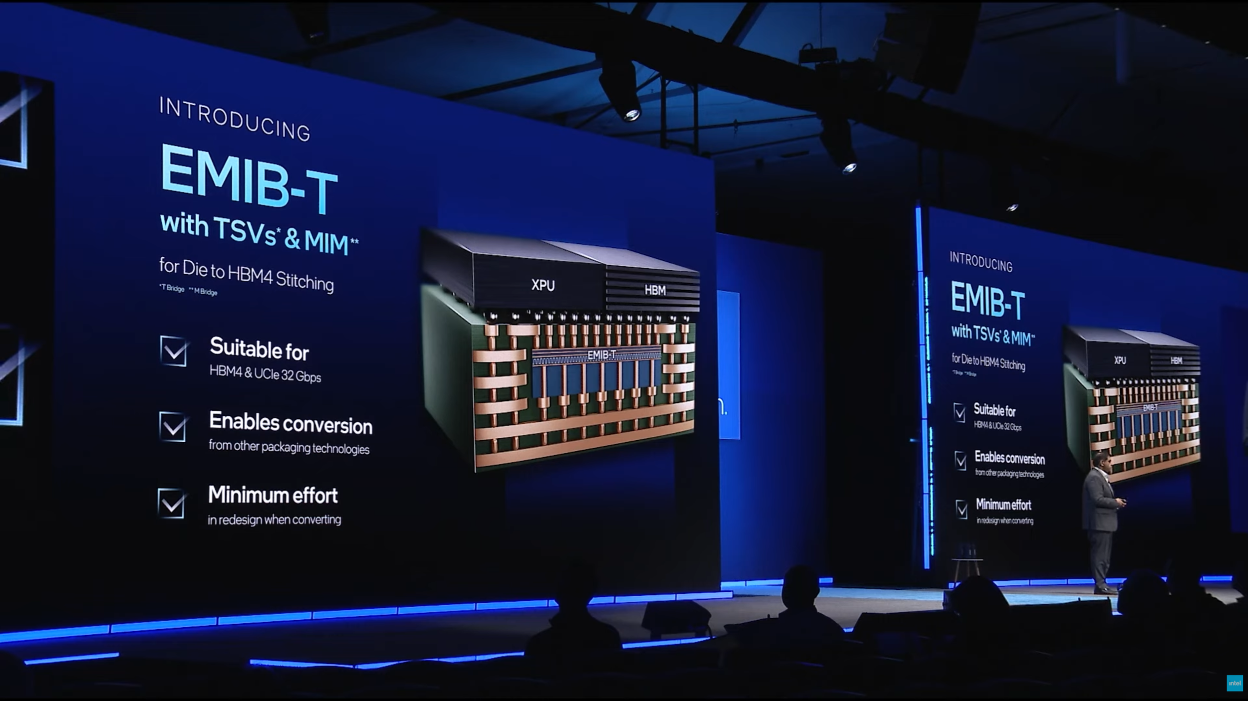
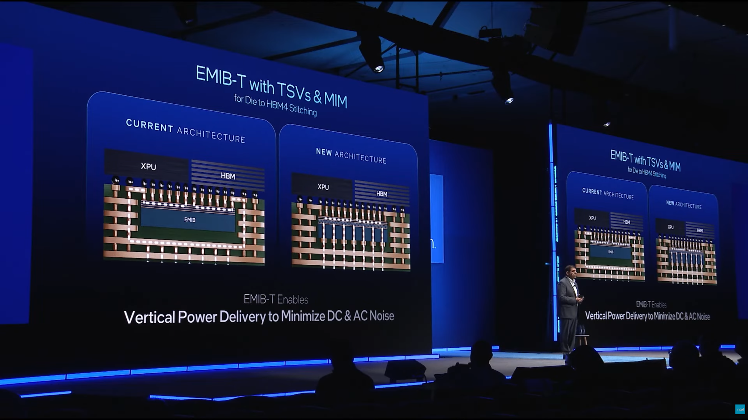
EMIB 2.5D is pitched as a cost effective method for connecting multiple complex dies, including logic to logic and logic to high bandwidth memory configurations. Intel also highlights specific extensions such as EMIB M with integrated capacitors and EMIB T with through silicon vias added to the bridge, positioning EMIB T as a way to ease integration with designs and IP flows originating from other packaging approaches.
EMIB 3.5D is described as combining EMIB with Foveros stacking in the same package, enabling broader heterogeneous integration and use cases where multiple 3D stacks need to coexist within one advanced system. Intel cites its data center GPU Max series system on chip as an example of how far this can scale, emphasizing extreme tile counts and very large transistor totals as proof points for mass produced heterogeneous packaging.
Intel summarizes its EMIB advantages around 3 themes it wants customers and partners to remember: normal package yield ranges, cost saving opportunities, and a design process that is simpler to execute than large interposer based solutions.
This packaging narrative plugs directly into Intel’s broader effort to attract foundry customers and strengthen its competitiveness as more advanced designs move toward multi die architectures. Intel is effectively betting that advanced packaging can be a differentiator customers choose for system level outcomes, not just for raw transistor density. If Intel can align EMIB and Foveros capabilities with a credible manufacturing roadmap, the company can offer an end to end story that competes on platform delivery, not only wafer fabrication.
For hardware enthusiasts and gamers watching from the sidelines, the long term payoff is that better packaging can translate into higher bandwidth die to die links, larger effective compute footprints, and more scalable designs that can power future server infrastructure, which eventually flows downstream into better content delivery, faster services, and more capable AI assisted features across gaming ecosystems.
What do you think will matter more over the next 2 years for advanced chips, process node leadership, or packaging leadership that enables bigger chiplet systems at reasonable cost?