
Intel EMIB T Pushes AI Packaging Beyond 10 Reticle Dies With 12 Gb/s HBM4e Support
Intel Foundry has presented its latest EMIB T advanced packaging developments at the 2026 IEEE Electronic Components and Technology Conference, outlining a path toward increasingly large AI and high performance computing packages that combine extensive chiplet integration, vertical power delivery, and next generation HBM connectivity.
According to the Intel Foundry ECTC 2026 overview, the company has reduced the first layer interconnect bump pitch of EMIB T to 25 µm, expanded supported package dimensions to 120 × 120 mm, and demonstrated the ability to integrate more than 9 reticle areas of compute and memory silicon inside a single package. Intel also reported signaling performance exceeding 12 Gb/s for HBM4e and 64 Gb/s for UCIe interfaces.
These developments arrive as AI accelerators and high performance computing processors require more compute tiles, HBM stacks, networking components, and specialized I O dies to operate within the same package. Conventional monolithic scaling cannot economically provide all of this silicon through a single die, making heterogeneous integration one of the semiconductor industry’s most important development areas.
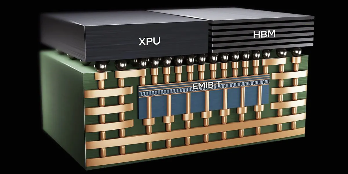
EMIB, or Embedded Multi Die Interconnect Bridge, connects neighboring dies through small silicon bridges embedded inside an organic package substrate. Unlike packaging architectures that use a large silicon interposer beneath the entire die complex, EMIB places high density silicon only where direct connections are required. This can reduce the total amount of silicon used for interconnect while allowing designers to combine chiplets produced through different process technologies.
EMIB T expands this architecture by integrating through silicon vias into the bridge. These vertical connections allow power and signals to travel directly through the embedded bridge instead of relying entirely on longer routing paths around it. Intel says this approach improves power delivery density and signal integrity, which become progressively harder to maintain as package dimensions, chiplet counts, and HBM requirements increase.
The company’s EMIB T scaling research describes package form factors larger than 120 × 120 mm and integration of more than 9 reticles of compute and memory content. Intel says the roadmap is intended to give architects the ability to build increasingly complete systems inside a single package while maintaining the bandwidth and power characteristics required by future AI and HPC platforms.
Intel also presented dedicated research titled Enabling 12+ Gb/s HBM4E with EMIB T Advanced Packaging Technology. The work focuses on the signal integrity, power integrity, routing density, and integrated power delivery required for future HBM4e interfaces. Electrical measurements and modeling reportedly confirmed operation beyond 12 Gb/s, positioning EMIB T as a potential packaging option for processors that will depend on substantially higher memory bandwidth than current HBM3e based accelerators.
This capability could become strategically important as advanced packaging and HBM availability increasingly influence how quickly new AI processors can enter volume production. The performance of an accelerator is no longer determined only by its compute architecture or manufacturing node. Package size, memory proximity, interconnect density, thermal management, power delivery, and manufacturing yield are becoming equally decisive platform constraints.
Intel and Siliconware Precision Industries also demonstrated the 3D integration of an SRAM chiplet inside a fan out embedded bridge package. The prototype achieved a bandwidth density of 265 GB/s/mm² while consuming less than 0.24 pJ/bit during balanced read and write workloads. At a reduced operating frequency, energy consumption reached 0.15 pJ/bit while maintaining 166 GB/s/mm² of bandwidth density.
The SRAM chiplet was connected vertically to a system on chip through a dense 25 µm microbump matrix. Intel reported that the die to die connection represented less than 15% of total power consumption, while data movement inside the dies accounted for approximately 30%. The result demonstrates how memory functions could be moved into embedded dies positioned close to compute logic, creating another path for improving bandwidth efficiency and reducing data movement energy.
Another Intel study, Package Architectures for Hyper Large Form Factors for AI and HPC Segment, examines package dimensions reaching as much as 240 × 240 mm. The proposed architectures combine ASICs, HBM, and I O dies while addressing connectivity between compute tiles, memory interfaces, 448G SerDes links, off package communication, power integrity, thermal management, mechanical reliability, and manufacturing yield.
Reaching that scale introduces significant engineering challenges. Large substrates are more vulnerable to warpage, uneven thermal expansion, power distribution losses, assembly defects, and encapsulation problems. Intel therefore presented separate research covering the encapsulation of ultra large die complexes.
The research includes case studies involving EMIB packages containing 5 times and more than 10 times the conventional reticle die area, along with Foveros assemblies exceeding 4 times the reticle area. Intel says improved material formulations, manufacturing equipment, and process development enabled void free encapsulation across these large structures.
This distinction is important. Intel’s current EMIB T scaling paper describes more than 9 reticles of compute and memory silicon inside a 120 × 120 mm package, while the encapsulation research demonstrates manufacturing processes for EMIB complexes exceeding 10 reticle areas. Intel’s broader roadmap extends the technology further, with the company targeting die complexes larger than 12 reticles by 2028.
Intel previously stated that EMIB T would move beyond 8 reticles during 2026 and exceed 12 reticles by 2028, potentially reaching approximately 10,000 mm² of silicon content while supporting at least 16 HBM4 or HBM5 stacks and 30 or more EMIB T bridges.
EMIB T is part of a broader Intel packaging portfolio that also includes EMIB M. EMIB M integrates metal insulator metal capacitors inside the silicon bridge to reduce electrical noise and improve power integrity. EMIB T introduces through silicon vias for direct vertical power and signal delivery, making it more suitable for extremely large AI processors with demanding HBM interfaces and dense chiplet layouts.
Both technologies are designed to connect logic dies and high bandwidth memory without requiring every component to be manufactured on the same process node. This process and intellectual property flexibility allows accelerator designers to combine compute, cache, networking, memory controllers, and I O functions from different manufacturing sources inside one package.
Intel has been producing EMIB based products since 2017, but AI infrastructure is giving the technology a significantly larger commercial opportunity. The company is already positioning EMIB T as one of its strongest differentiators against competing advanced packaging platforms, particularly where customers require larger package dimensions, additional HBM stacks, flexible chiplet sourcing, or an alternative to constrained packaging capacity.
That opportunity is also connected to recent industry speculation around future NVIDIA platforms, Rubin Ultra design could use Intel EMIB T. NVIDIA and Intel have not confirmed such a packaging agreement, but the discussion demonstrates why EMIB T is receiving increasing attention as AI processors move toward larger multi chip designs. Google has also reportedly evaluated Intel manufacturing and packaging technologies for future AI silicon. The EMIB could provide hyperscale customers with another option for integrating internally designed accelerators without depending entirely on a full silicon interposer architecture.
Advanced substrates will become another component of this scaling strategy, Intel backed glass substrate packaging could improve mechanical stability, signal integrity, dimensional control, and package size as AI processors continue moving beyond the practical limits of traditional organic substrates.
Intel’s most credible AI opportunity may not begin with replacing TSMC as the primary manufacturer of leading edge accelerator dies. It may begin by becoming one of the industry’s most valuable advanced packaging partners.
EMIB T addresses a real infrastructure constraint. AI processors require larger die complexes, more HBM stacks, better power delivery, and denser chiplet connections, but full interposer solutions become increasingly complicated and expensive as package dimensions expand. Intel’s embedded bridge approach provides an alternative that concentrates high density silicon interconnects only where they are needed.
The ECTC 2026 results show that EMIB T is advancing beyond a conceptual roadmap. Intel has demonstrated 25 µm interconnect pitches, package dimensions of 120 × 120 mm, more than 9 reticles of integrated silicon, 12 Gb/s HBM4e signaling, 64 Gb/s UCIe connectivity, and encapsulation methods for EMIB complexes exceeding 10 reticle areas.
However, laboratory demonstrations and technical papers are only part of the equation. Intel must also prove competitive cost, manufacturing yield, substrate availability, thermal performance, assembly throughput, and reliable volume production. Those factors will determine whether EMIB T becomes a widely adopted external foundry platform or remains primarily associated with selected Intel products.
The strategic potential is substantial. If AI accelerator companies need a second advanced packaging supply chain alongside established providers, Intel already has one of the few technologies technically capable of entering that conversation. EMIB T may therefore become one of the most important assets in Intel Foundry’s attempt to rebuild its relevance in the AI era.
Could advanced packaging become Intel’s strongest path back into the AI market, or will established packaging ecosystems remain too difficult to challenge?
