
Intel Completes RAMP C and Advances Domestic 18A Defense Production
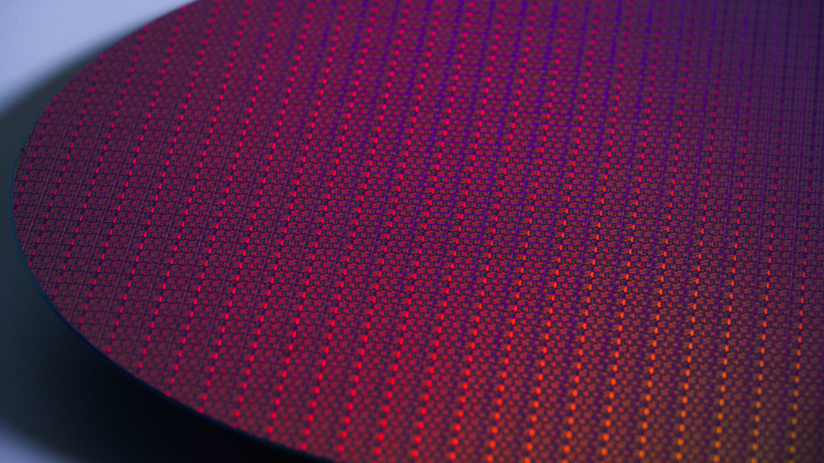
Intel Foundry has completed the Rapid Assured Microelectronics Prototypes Commercial program, known as RAMP C, establishing a pathway for commercial companies and the United States defense industrial base to design, prototype, and manufacture advanced semiconductors domestically.
The program began in 2021 through cooperation between Intel and the United States Department of War. According to the official Intel RAMP C announcement, its objective was to develop a domestic ecosystem for leading edge CMOS technology, including intellectual property, design tools, process access, prototype validation, and secure manufacturing infrastructure.
RAMP C progressed through 3 main phases. The first established the technology, intellectual property, and design tools needed to prepare customers for test chip tapeouts. The second expanded the available ecosystem and introduced additional commercial and defense customers to Intel 18A. The final phase supported the tapeout and testing of early defense product prototypes, demonstrating that participating designs could progress toward secure production at larger manufacturing volumes.
"RAMP C enables commercial companies and the defense industrial base to design and fabricate trusted microelectronics onshore."
— Quote by: Eric Makara, Program Manager for Microelectronics, OUSW(R&E)
The completion of RAMP C does not mean every participating semiconductor has immediately entered mass production. Instead, it confirms that Intel has created and validated the design infrastructure required to move compatible projects from early development into production readiness. Customers can now continue that transition through Secure Enclave, Intel’s protected manufacturing framework for sensitive government and mission critical chips.
Intel describes itself as the only United States company that researches, develops, and manufactures leading edge semiconductor technology domestically. While international manufacturers operate fabrication facilities inside the country, Intel remains uniquely positioned as a United States headquartered company controlling both advanced process development and domestic production.
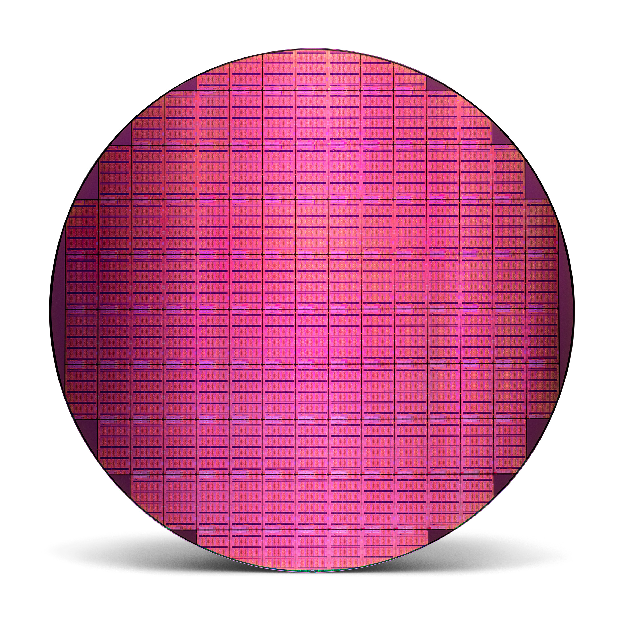
Intel 18A is central to this strategy. The process introduces RibbonFET gate all around transistors and PowerVia backside power delivery, technologies designed to improve performance, power efficiency, routing, and transistor density. Intel states that its growing high volume 18A manufacturing capacity provides the scalable foundation needed to produce trusted advanced microelectronics inside the United States.
The company has already used Intel 18A for Panther Lake processors, while its broader foundry roadmap continues with Intel 18A P and Intel 14A. Intel 18A P recently entered risk production, bringing improvements in transistor performance, interconnect resistance, and thermal efficiency while maintaining design rule compatibility with standard Intel 18A.
Intel has also become the first manufacturer to incorporate selected High NA EUV layers into a shipping high volume logic product through Panther Lake production. Together, these developments strengthen Intel’s argument that its domestic manufacturing infrastructure can support advanced commercial processors, artificial intelligence hardware, aerospace systems, and secure government silicon.
Secure Enclave will extend the work established through RAMP C by providing protected domestic design, fabrication, and advanced packaging capabilities. Intel says the program will support mission critical systems operating under strict size, weight, power, security, and supply chain requirements. This includes applications such as radar, infrared sensing, aerospace computing, tactical edge processing, and other systems that require advanced silicon without relying on overseas manufacturing.
Completing RAMP C is an important strategic milestone, but Intel’s real test begins with production scale. Prototype access and validated design tools provide a credible foundation, yet government and commercial customers will ultimately evaluate Intel Foundry through yield stability, manufacturing cost, delivery consistency, security, and long term process support.
Intel’s strongest advantage is not only that 18A is technically advanced. It is that the company can combine process development, wafer fabrication, packaging, and secure manufacturing within a domestic supply chain. That position could make Intel increasingly important to United States semiconductor policy even before its external foundry business becomes financially competitive with TSMC.
Can secure domestic production make Intel Foundry a serious alternative to overseas leading edge manufacturing, or will yield and cost remain the deciding factors?
