
ASML High NA EUV Enters Volume Production With Intel Panther Lake
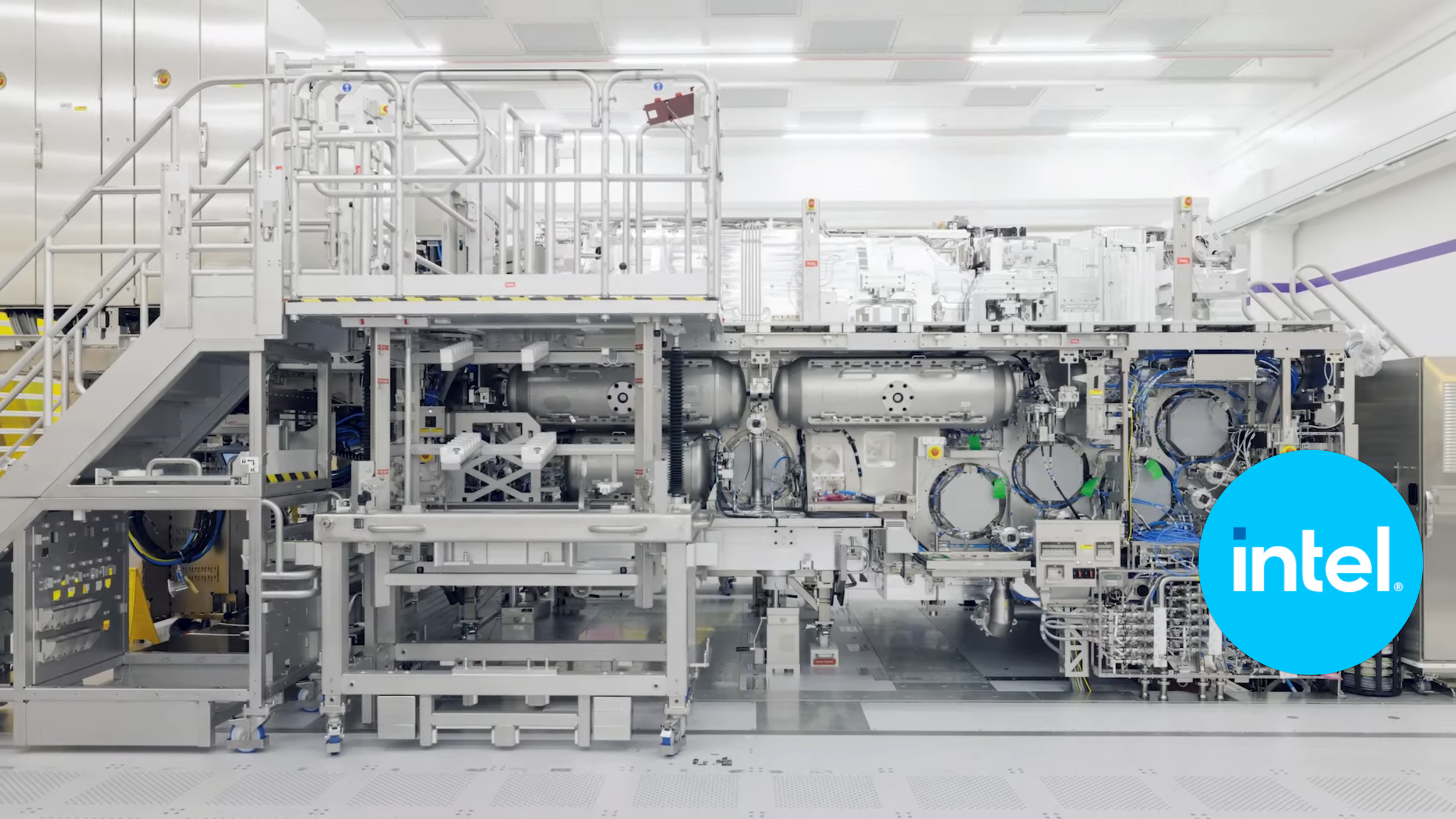
ASML has confirmed that its High NA EUV lithography technology is now being used in high volume logic manufacturing for the first time, with Intel Foundry applying the equipment to selected Intel 18A layers used in a subset of Intel Core Ultra Series 3 processors, codenamed Panther Lake.
According to the official ASML announcement, products manufactured with these qualified High NA EUV processes are already shipping to customers. ASML describes Panther Lake as the first high volume logic product to incorporate the technology, giving Intel an important manufacturing milestone as it continues expanding Intel 18A production.
The announcement does not mean every Panther Lake processor or every Intel 18A layer is manufactured using High NA EUV. Intel has qualified the technology on selected layers for a subset of Core Ultra Series 3 products. Those layers are dual qualified across ASML High NA EXE equipment and the company’s established NXE EUV platform, providing greater production flexibility while Intel and ASML collect manufacturing data related to system configuration, uptime, process control, and yield.
ASML says yields achieved through the High NA process option now match those delivered by its NXE platform. This is an important readiness signal because new lithography equipment must demonstrate consistent output and manufacturing reliability before semiconductor companies can introduce it across larger portions of their production roadmaps.
“The introduction of High NA EUV marks a substantial development in semiconductor lithography.
— Christophe Fouquet, ASML President and CEO
Intel installed the first commercial High NA EUV system at its Hillsboro, Oregon, research and development facility in 2024. The company was also the first chipmaker to install and complete acceptance testing of ASML’s second generation TWINSCAN EXE:5200B system, which improves output, overlay accuracy, and light source performance compared with the earlier EXE:5000 platform.
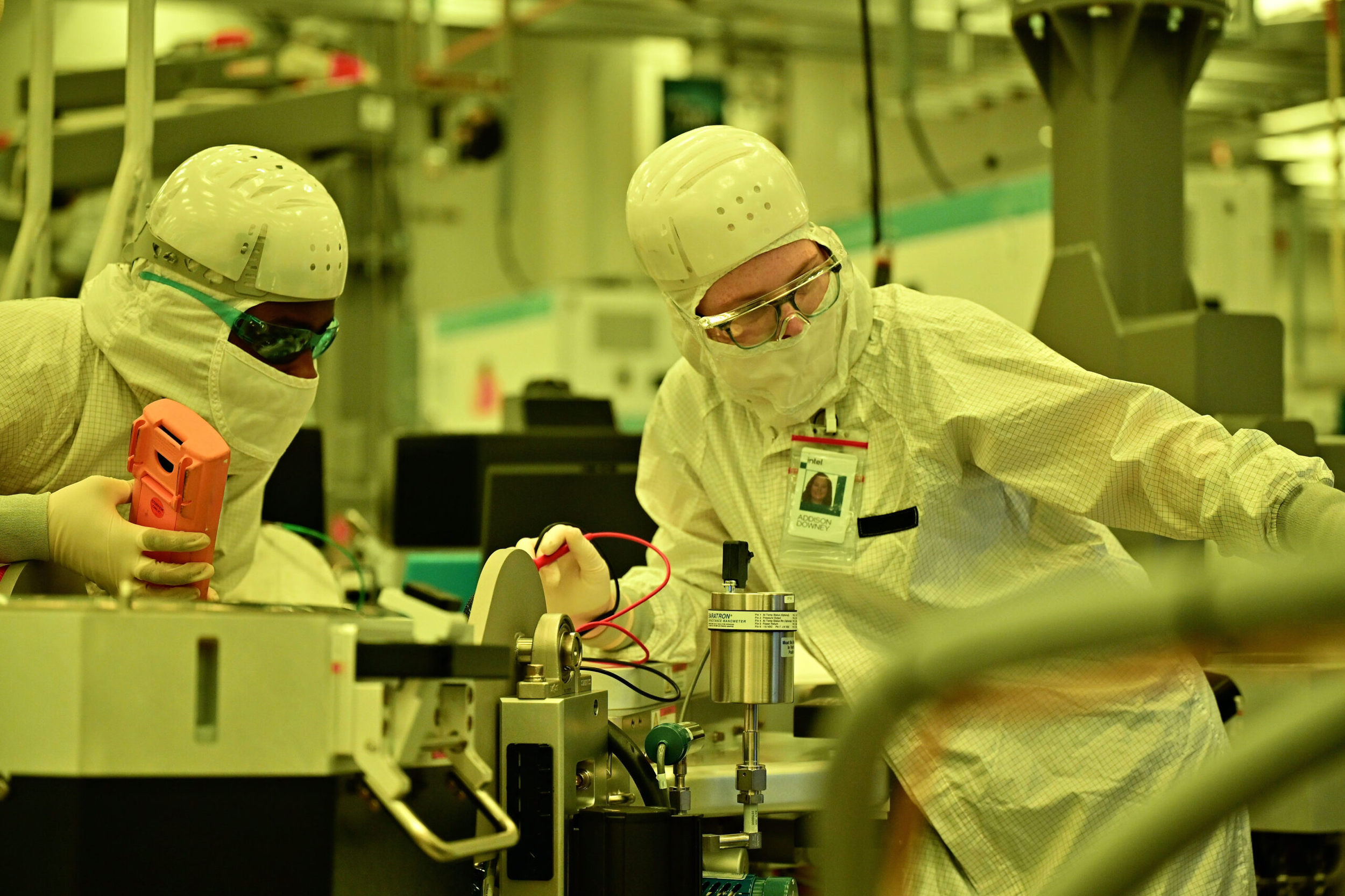
The EXE:5200B uses a numerical aperture of 0.55 and is designed to support volume manufacturing for advanced logic processes below 2 nm alongside leading memory technologies. Its increased resolution allows manufacturers to print smaller and denser semiconductor structures with fewer patterning steps, potentially improving process simplicity, cycle time, and manufacturing flexibility.
“High NA EUV can be integrated into advanced semiconductor manufacturing at scale.
— Naga Chandrasekaran, Executive Vice President and General Manager of Intel Foundry”
Panther Lake is Intel’s first client system on chip produced using Intel 18A, which combines RibbonFET gate all around transistors with PowerVia backside power delivery. Intel previously confirmed that Panther Lake entered production in 2025, with the main manufacturing ramp taking place at Fab 52 in Arizona. The newly qualified High NA layers are being produced through Intel’s Oregon development and manufacturing infrastructure.
The milestone also strengthens the manufacturing foundation for future Intel processes. High NA EUV can be incorporated into upcoming nodes according to customer requirements, while the manufacturing information collected through Panther Lake should help Intel prepare the technology for broader use. This development follows Intel 18A P entering risk production.
Intel becoming the first company to ship a high volume logic product manufactured with High NA EUV is a meaningful technical victory, particularly as Intel Foundry works to rebuild confidence in its process execution.
The most important detail is not simply that Panther Lake uses the equipment. It is that selected layers have reached yields comparable to ASML’s established NXE platform while shipping inside commercial products. This moves High NA EUV beyond research wafers and process demonstrations into genuine consumer silicon.
The limited deployment also reflects a careful manufacturing strategy. Intel is not replacing its existing EUV fleet immediately. It is qualifying High NA where the technology provides value while retaining the ability to manufacture those layers through existing equipment. That reduces production risk and creates a practical path toward broader adoption on Intel 18A derivatives and future nodes.
Intel now holds first mover status in High NA logic production. The larger challenge will be converting that early technical advantage into stronger yields, competitive manufacturing costs, and external foundry customers.
Could Intel’s early adoption of High NA EUV provide a lasting manufacturing advantage, or will its competitors quickly close the gap once the technology reaches wider production?
