
Intel Claims It Is Only a Few Percent Behind TSMC as High NA EUV Becomes Key to 14A
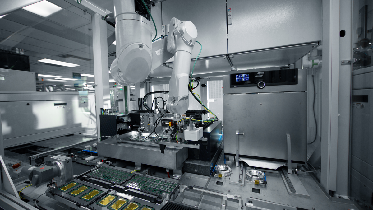
Intel believes its semiconductor manufacturing technology has nearly caught up with TSMC, although matching the Taiwanese foundry's enormous production capacity will take considerably longer. During an extensive interview with Dwarkesh Patel, Intel Chief Technology Officer Pushkar Ranade argued that the company is now within a few percentage points of its main competitor in performance, power efficiency and transistor density, emphasizing that manufacturing execution matters more than small technological differences.
Ranade acknowledged that TSMC maintains a substantial advantage in wafer production volume, but argued that Intel's immediate challenge is achieving consistent manufacturing yields and predictable production schedules. He explained that semiconductor fabrication facilities have approximately 80% fixed costs, making higher utilization and improved yields essential for competing economically.
"You can be off by a few percent, but you need to be on time."
— Quote by: Pushkar Ranade, Intel CTO
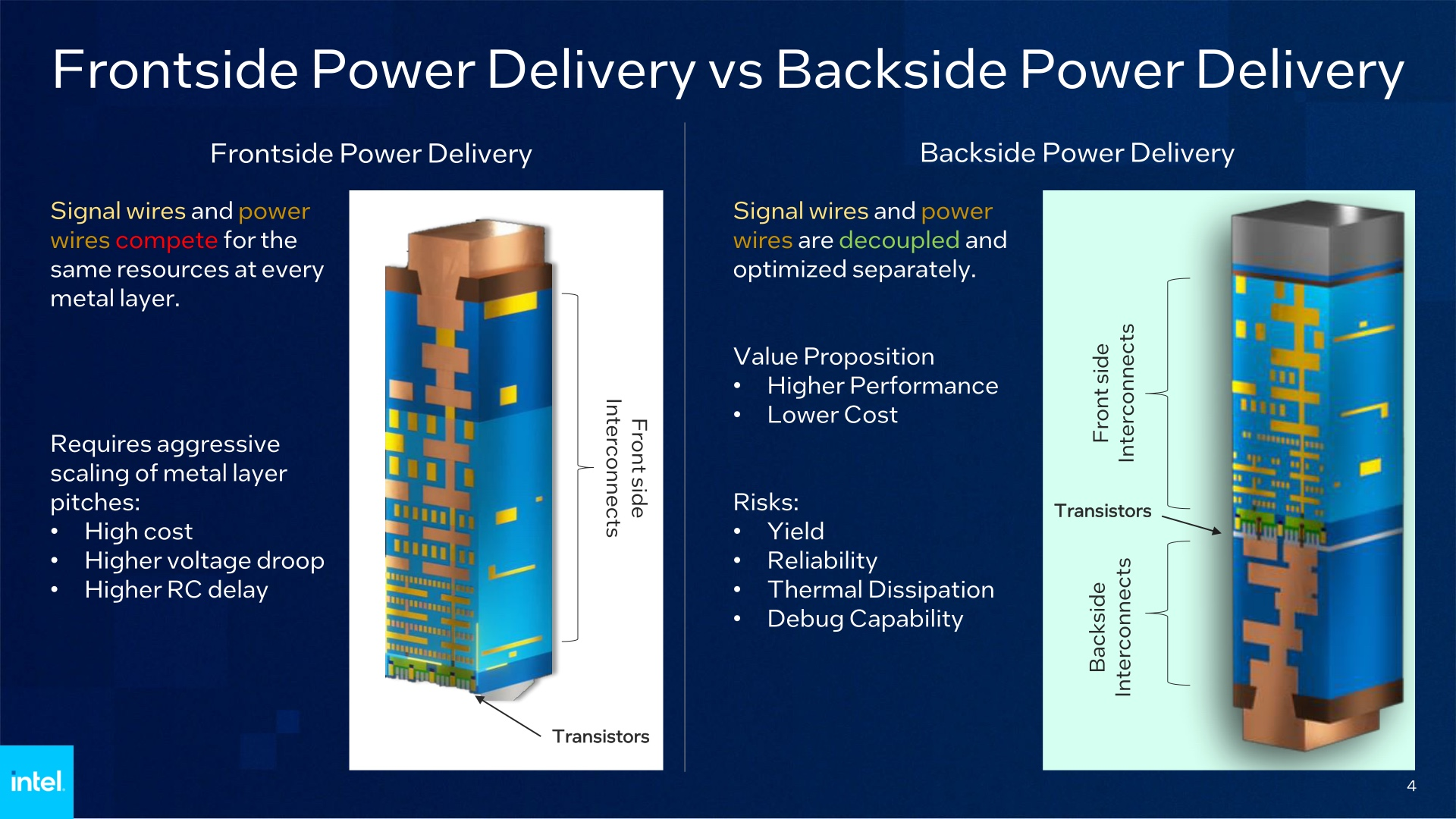
The discussion also highlighted Intel's aggressive investment in High Numerical Aperture Extreme Ultraviolet lithography, commonly known as High NA EUV. Chris Auth, Intel Vice President and General Manager of Manufacturing Development and Customer Engagement, explained that the company's backside power delivery architecture provides an important manufacturing advantage by moving power connections behind the silicon wafer. This frees additional space for signal routing and allows certain structures to be printed using High NA EUV without requiring multiple patterning steps.
High NA EUV uses a numerical aperture of 0.55 compared with 0.33 for conventional EUV, providing approximately 1.7 times greater single exposure resolution. Although these systems are substantially more expensive, reducing the number of exposures could improve manufacturing efficiency and lower defect opportunities.
Intel vs TSMC Manufacturing Strategies
| Technology | Intel Foundry | TSMC |
|---|---|---|
| Advanced Process | Intel 18A / 14A | N2 / A16 / A14 |
| Transistor Technology | RibbonFET | Nanosheet |
| Backside Power | PowerVia / PowerDirect | Super Power Rail on A16 |
| EUV Strategy | Early High NA adoption | Primarily conventional EUV |
| Next Major Node | Intel 14A in 2028 | TSMC A14 in 2028 |
| Manufacturing Advantage | Advanced process integration | Greater production scale |
The processes are not directly equivalent. Manufacturing technologies, production maturity and performance characteristics differ between companies.
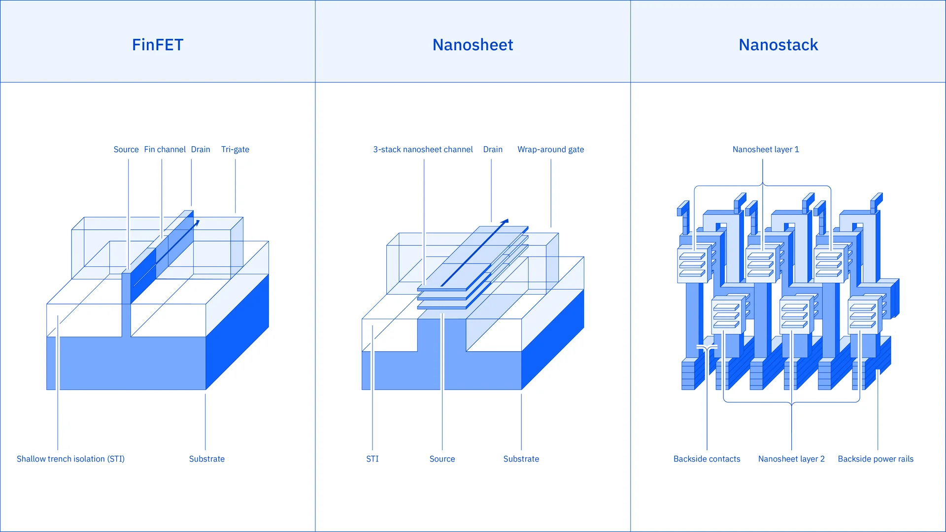
According to Auth, Intel's 14A process offers High NA EUV as an option within its Process Design Kit (PDK), with adoption determined through individual customer discussions. However, TSMC is also introducing backside power delivery through its A16 technology, meaning Intel's architectural distinction does not necessarily represent a permanent technological advantage.
Intel has already demonstrated progress with High NA EUV beyond experimental research. In September 2026, ASML confirmed that Intel had processed more than 1 million wafers across development, qualification and production activities, including selected layers on a subset of Panther Lake processors manufactured using Intel 18A.
Looking ahead, Intel Foundry expects its 14A process to deliver 15% to 20% higher performance at equivalent power, or 25% to 35% lower power at equivalent performance, compared with Intel 18A. The company also targets up to 30% greater chip density, supported by second generation RibbonFET transistors and PowerDirect backside power delivery.
These developments follow Intel's reported progress in reducing 14A manufacturing defects, with high volume production currently targeted for 2028. TSMC plans to introduce A14 during the same year, setting up another major competition in advanced semiconductor manufacturing.
Nevertheless, technological competitiveness does not automatically translate into market leadership. Intel must secure external customers, demonstrate reliable yields and expand production capacity while competing against TSMC's established manufacturing ecosystem. Ranade's estimate of a small technology gap remains Intel's own assessment rather than an independently verified comparison across equivalent manufacturing processes.
Intel's strongest opportunity lies in combining competitive transistor technology with a manufacturing architecture designed around future lithography advancements. High NA EUV and backside power delivery could offer meaningful advantages as semiconductor designs become increasingly complex, particularly for AI accelerators and high performance processors.
However, TSMC's competitive advantage extends far beyond transistor specifications. Its established customer relationships, production capacity and manufacturing consistency remain difficult to replicate. For Intel, successfully commercializing 14A will be more important than claiming a marginal performance advantage. If the company can demonstrate reliable high volume production while attracting major external chip designers, the semiconductor industry could finally gain a more competitive alternative to TSMC at the leading edge.
Do you believe Intel's High NA EUV strategy and 14A process can challenge TSMC's manufacturing dominance, or will TSMC's production scale and established customer relationships remain the decisive advantages?
