
Intel 14A2 May Add Dual Side Power Delivery as 21 nm M0 Scaling Raises Interconnect Pressure
Intel may be preparing a more complex power delivery strategy for its future 14A2 manufacturing process, as the company pushes deeper into angstrom class scaling while trying to close the density gap against TSMC and Samsung Foundry. According to a report from ETNews, Intel is evaluating dual side power delivery for the second version of its 14A process because tighter metal interconnect dimensions could create new voltage drop and resistance challenges. The report says the standard 14A process targets an M0 pitch of around 28 nm, while 14A2 could reduce that figure to around 21 nm.
M0 pitch refers to the spacing between the lowest metal interconnect lines used to move signals between transistors. Shrinking this pitch can improve density because more logic can fit into a smaller area, but it also increases manufacturing difficulty and electrical resistance. That is why advanced nodes are becoming less about transistor scaling alone and more about the full stack of lithography, power routing, signal routing, interconnect resistance, voltage stability, and thermal management.
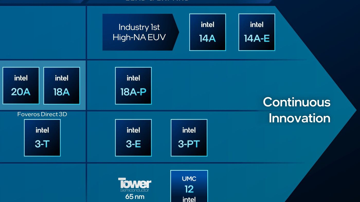
Intel’s official 14A process page already lists RibbonFET 2 gate all around transistors, PowerDirect back side power delivery, Turbo Cells, up to 30% chip density improvement versus Intel 18A, 15% to 20% higher performance at the same power, or 25% to 35% lower power at the same performance. These are important claims because 14A is not just another internal Intel node. It is one of the company’s most important attempts to become a credible external foundry competitor for AI, client, mobile, and data center silicon.
The reported 14A2 challenge comes from the tradeoff between density and power integrity. Back side power delivery is designed to move power rails away from the transistor signal routing side, freeing space and reducing congestion. However, as interconnects become smaller and resistance rises, the current delivery path may become harder to manage with back side routing alone. ETNews reports that Intel is considering adding front side power support as well, creating a dual side delivery structure to stabilize voltage and reduce drop across the chip.
This would not be a simple design choice. Dual side power delivery can improve flexibility, but it also increases process complexity, design rules, verification work, and potential manufacturing cost. Intel is already expected to use High NA EUV tools with 14A, and Intel CFO David Zinsner previously said 14A would carry higher wafer cost than 18A because of that equipment choice. Tom’s Hardware reported that High NA EUV tools can cost around $380 million per unit, compared with around $235 million for current Low NA EUV tools, making customer volume critical for the economics of Intel’s foundry roadmap.
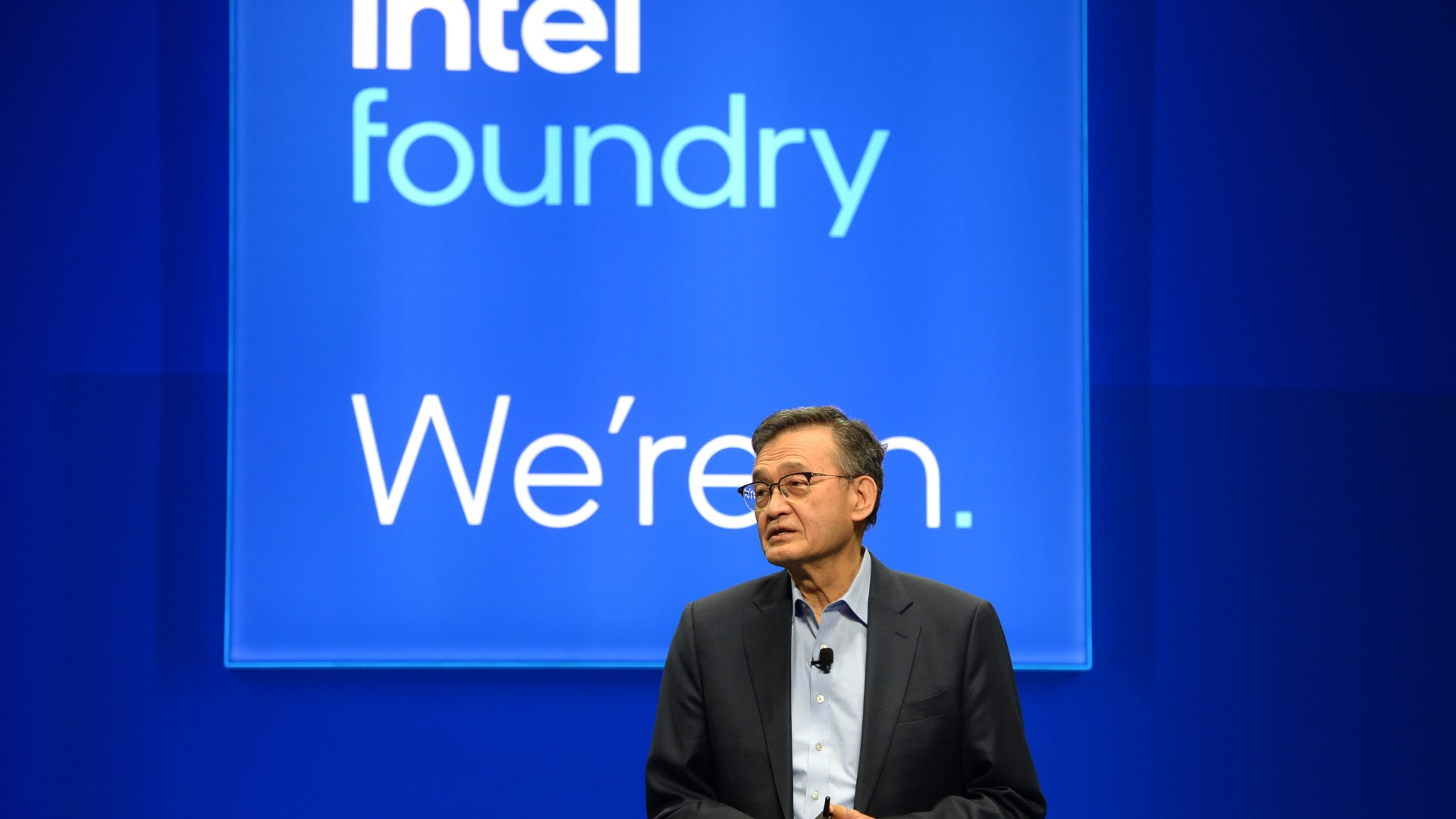
Intel is also racing the clock on customer adoption. The Elec reported that Intel plans to begin external distribution of its 14A 0.9 process design kit in October 2026, while targeting mass production in 2029 after customer discussions on product scale and design requirements. Reuters previously reported that Intel had attracted interest from customers for 14A test chips and that CEO Lip Bu Tan had publicly committed to improving Intel Foundry after taking over leadership.
The competitive pressure is intense. TSMC’s official A14 technology page describes A14 as its next cutting edge logic process after N2, with dimensional scaling intended to deliver full node gains in power, performance, and area. TSMC has also previewed A12, an A14 platform enhancement that adds Super Power Rail back side power delivery for AI and HPC applications, with production planned for 2029.
Samsung is moving in the same direction. At Samsung Foundry Forum 2024, the company announced SF2Z as part of its 2 nm roadmap, while TrendForce reported that SF2Z uses optimized back side power delivery to improve power, performance, area, IR drop, and HPC design behavior compared with Samsung’s first generation SF2 node.
That makes power delivery one of the central battlegrounds in the next phase of semiconductor scaling. Intel has PowerVia and PowerDirect, TSMC has Super Power Rail, and Samsung has its back side power delivery network for SF2Z. The question is no longer whether advanced foundries need back side power. The question is how far each company can push density before power routing, interconnect resistance, and patterning complexity force another architectural adjustment.
Intel 18A P entering risk production with Power Boost and dual contact transistor design, where Intel used PowerVia to improve transistor drive current, thermal resistance, via resistance, and voltage behavior. That context matters because 18A P is effectively Intel’s bridge between today’s PowerVia implementation and the larger 14A leap. If 14A2 truly requires dual side power delivery, it shows that each generation of scaling now demands deeper co optimization across transistor, interconnect, power, and layout design.
Intel’s reported 14A2 direction shows how difficult the angstrom era is becoming. Shrinking M0 pitch from 28 nm to 21 nm may sound like a straightforward density improvement, but it changes the electrical behavior of the chip. Smaller wires increase resistance, voltage delivery becomes more fragile, and power routing has to be redesigned around new physical limits.
This is why Intel’s foundry comeback is not only a matter of having advanced tools. High NA EUV can help pattern smaller features, but it also raises cost and manufacturing complexity. PowerDirect can improve back side delivery, but 14A2 may still need front side support to handle voltage drop and interconnect resistance. Density gains are valuable only if they can be manufactured reliably and delivered to customers with predictable design rules.
The bigger competitive story is that Intel, TSMC, and Samsung are all reaching the same conclusion from different roadmaps. Advanced logic is becoming a power delivery problem as much as a transistor problem. The foundry that wins will not simply be the one with the smallest number. It will be the one that delivers stable yield, strong design enablement, better power integrity, and customer confidence at scale.
For Intel, 14A2 could become a powerful technical showcase, but only if it arrives with mature tools, committed customers, and a realistic cost structure. The technology ambition is clear. The execution window is much tighter.
Can Intel’s 14A and 14A2 roadmap help it close the foundry gap with TSMC and Samsung, or will power delivery complexity make the race even harder?
