
3D X DRAM Moves Closer to Reality as a High Density HBM Alternative for AI Memory
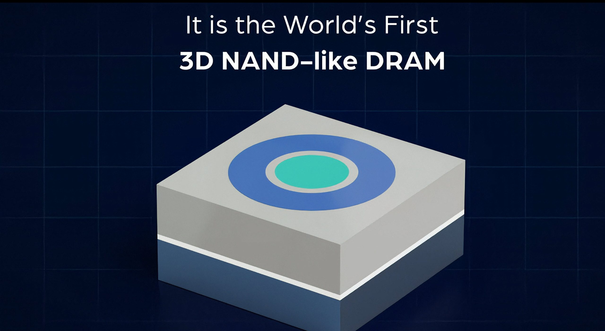
NEO Semiconductor’s 3D X DRAM technology is moving one step closer to reality, bringing renewed attention to a memory architecture designed to address one of the biggest limitations in modern AI and HPC systems: memory density. Originally announced in 2023, 3D X DRAM was introduced as a new DRAM architecture that borrows concepts from 3D NAND style vertical scaling to overcome the capacity limits of traditional DRAM.
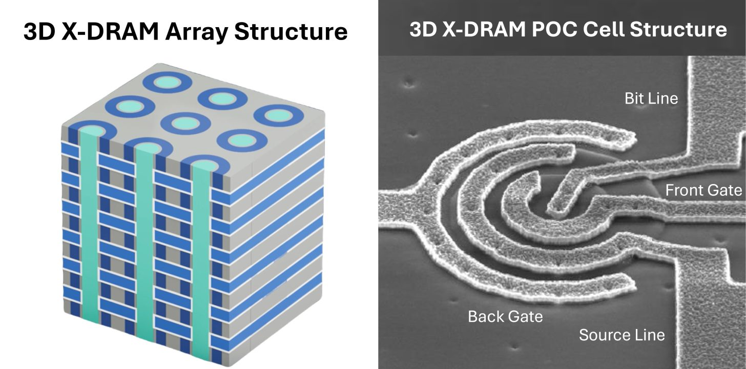
The company later unveiled multiple IGZO based 3D X DRAM cell designs, including 1T1C and 3T0C structures, with the goal of delivering much higher density, lower power consumption, and better scalability for AI, edge computing, in memory processing, and next generation high bandwidth memory solutions.
At the heart of NEO Semiconductor’s proposal is a simple but ambitious idea: instead of stacking multiple DRAM dies like HBM, 3D X DRAM aims to build multiple DRAM layers inside a monolithic like single die structure. This could potentially reduce complexity, improve density, and make manufacturing easier by using infrastructure and process concepts closer to existing 3D NAND production.
The timing is important. AI and HPC systems are placing enormous pressure on memory supply, especially HBM. While HBM remains the leading memory solution for AI accelerators, it is expensive, complex to manufacture, difficult to scale quickly, and requires extensive testing and validation before being deployed on advanced server chips. That makes alternatives like 3D X DRAM particularly interesting, especially if they can offer higher density while reducing cost and production complexity.
NEO Semiconductor’s 3D X DRAM technology includes several different cell variants, each targeting different use cases.
1T1C, or one transistor and one capacitor, is positioned as the core solution for high density DRAM. It is designed to remain compatible with mainstream DRAM and HBM roadmaps, making it the most direct candidate for future high density memory products.
3T0C, or three transistors and zero capacitors, is optimized for current sensing operations and is aimed at AI workloads and in memory computing. This design could be especially relevant as AI systems increasingly look for ways to reduce data movement between compute and memory.
1T0C, or one transistor and zero capacitors, uses a floating body cell structure and is intended for high density DRAM, in memory computing, hybrid memory, and logic related architectures.
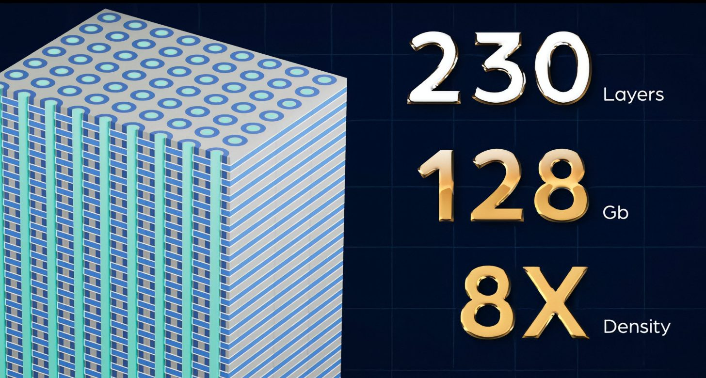
The company’s key claims focus on retention, efficiency, manufacturing scalability, bandwidth, and high performance access. Thanks to IGZO channel technology, NEO says its 1T1C and 3T0C simulations show retention times of up to 450 seconds, dramatically reducing refresh power compared with conventional DRAM behavior. TCAD simulations also reportedly confirm fast 10 nanosecond read and write speeds alongside long retention characteristics.
Manufacturing compatibility is another major part of the pitch. NEO says 3D X DRAM can use a modified 3D NAND process with minimal changes, which could allow it to scale more quickly than entirely new memory technologies. This is one of the most important claims because the memory industry is highly sensitive to yield, cost, and production readiness. A new architecture is only useful if it can eventually be manufactured at competitive scale.
Bandwidth is also central to the design. NEO says 3D X DRAM uses unique array architectures and hybrid bonding to improve memory bandwidth while lowering power consumption. For AI accelerators, this is critical. AI performance is often limited not only by raw compute, but by how quickly data can move between memory and processors. Any memory technology that improves density, bandwidth, and power efficiency at the same time would be highly valuable.
Now, NEO Semiconductor says it has demonstrated a 3D X DRAM Proof of Concept and secured additional investment to push the project forward. The proof of concept test chips reportedly show that 3D X DRAM can be manufactured using existing 3D NAND infrastructure, replacing the traditional horizontal DRAM scaling model with a vertically layered approach.
The first proof of concept test results are promising:
| Test Item | Result |
|---|---|
| Read and write latency | Less than 10 ns |
| Data retention | More than 1 second at 85°C |
| Bit line disturbance | More than 1 second at 85°C |
| Word line disturbance | More than 1 second at 85°C |
| Endurance | More than 10¹⁴ cycles |
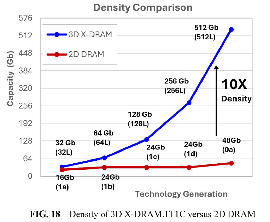
The data retention result is especially notable because NEO says it is 15 times better than the 64 ms JEDEC standard. Longer retention can reduce refresh frequency, which directly impacts power efficiency. In large AI systems, where memory power consumption becomes a major operating cost, reducing refresh overhead could provide meaningful benefits.
However, 3D X DRAM is still not a production ready HBM replacement. It remains in the development and proof of concept stage, and the memory market will need far more evidence before it can be considered a real commercial alternative. The key questions will be manufacturing yield, cost per bit, thermal behavior, bandwidth scaling, controller compatibility, packaging requirements, reliability, and whether major memory manufacturers are willing to adopt the technology.
Still, the progress is important because the AI memory problem is not going away. Model sizes, context windows, inference demand, agentic AI workloads, and HPC datasets are all increasing the need for more memory capacity and bandwidth. HBM will continue to dominate the high end accelerator market in the near term, but the industry clearly needs more options.
Intel is also preparing a similar class of next generation memory technology called ZAM, or Z Angle Memory, which is designed to offer high density, wide bandwidth, and lower power consumption for AI and HPC systems. Like 3D X DRAM, Intel’s ZAM remains far from mass production, but both technologies show that the semiconductor industry is actively searching for alternatives to today’s memory scaling limitations.
For AI hardware makers, the appeal is obvious. A memory technology that can offer higher density, strong bandwidth, lower power consumption, easier manufacturing, and better cost efficiency would directly address one of the most painful bottlenecks in the current AI boom. For consumers, the long term impact could also matter. If data center memory demand becomes easier to serve, it could eventually reduce pressure on the wider DRAM market, including PC memory and storage pricing.
NEO Semiconductor’s 3D X DRAM is still early, but it is becoming more than a paper concept. With proof of concept chips now demonstrated and investment secured, the technology has taken a meaningful step forward. The next challenge is turning promising test results into a scalable memory product that can compete in one of the most demanding markets in the semiconductor industry.
If 3D X DRAM can deliver on its promises, it could become one of the most important memory innovations of the AI era.
Do you think 3D X DRAM and ZAM can become real HBM alternatives, or will HBM remain the dominant memory solution for AI accelerators?