
Intel’s ZAM Memory Gets Major Support From Japan as a Potential Low Power HBM Alternative
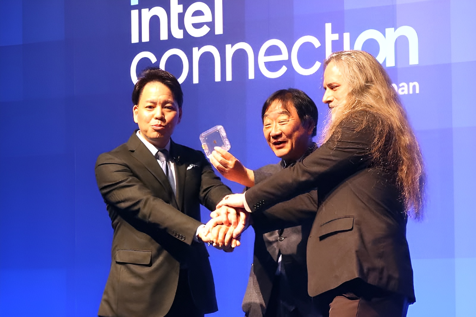
Intel’s next generation ZAM memory project has received a major boost from Japan, with Intel Kabushiki Kaisha and SoftBank subsidiary SAIMEMORY confirming that the technology has been selected by Japan’s New Energy and Industrial Technology Development Organization, also known as NEDO. The program will now receive government backed support, accelerating the development of ZAM as a new memory solution aimed at AI, HPC, and next generation compute markets.
According to Intel’s official announcement, the NEDO selection is designed to help advance ZAM toward broader development and future commercialization. The project is being positioned as a response to one of the biggest constraints in modern AI infrastructure: memory availability, bandwidth, density, and power consumption. As AI accelerators and HPC systems continue to demand more memory capacity and greater bandwidth, companies across the semiconductor industry are searching for alternatives and complements to today’s HBM technology.
ZAM, which stands for Z Angle Memory, was first introduced earlier this year as part of Intel’s collaboration with SoftBank. The goal is to create a new memory architecture that can deliver high density, wide bandwidth, and lower power consumption for advanced compute systems. With NEDO now backing the project, Intel and SAIMEMORY will be able to work with a wider network of technology, manufacturing, and supply chain partners in Japan and internationally.
ことしの年次イベントIntel Connection Japan 2026で発表した、SAIMEMORYと共同で推進している次世代メモリー開発が、NEDO(国立研究開発法人新エネルギー・産業技術総合開発機構)の助成事業に採択されました。
— インテル【公式】 (@IntelJapan) April 24, 2026
これにより、AI時代に向けた次世代積層DRAMアーキテクチャーであるZ-Angle Memory (ZAM)… pic.twitter.com/G8vE17gKb2
The timing is important. AI demand has placed enormous pressure on advanced memory supply, especially HBM. While HBM remains critical for current AI accelerators, the industry is already looking ahead to architectures that can reduce power, improve density, simplify manufacturing, and support larger memory pools close to compute silicon. Intel’s ZAM is being developed to address that future need.
“Intel has spent years proving the science behind ZAM, from DOE national laboratories to our Next Generation DRAM Bonding initiative. We believe this award puts that work on a fast track to global deployment and strengthens the kind of U.S. Japan technology partnership that will matter enormously in the years ahead.
Quote by: Makoto Ohno”
From a technical perspective, ZAM is designed to deliver 40% to 50% lower power consumption while supporting much higher memory density. Intel has described the architecture as a simplified design that could make manufacturing easier compared with some existing advanced memory approaches. The technology is also being discussed with potential densities of up to 512GB per chip, which would represent a significant leap for memory capacity in AI and HPC systems.
The core idea behind Z Angle Memory is the use of tightly stacked DRAM ICs connected through Z Angle interconnects. These stacks would then connect to the main compute chip through Intel’s EMIB technology under the base die. EMIB, or Embedded Multi Die Interconnect Bridge, is one of Intel’s key advanced packaging technologies, allowing different chiplets or dies to communicate with high bandwidth while avoiding some of the complexity of full silicon interposers.
This packaging direction matters because the future of AI hardware is increasingly tied to advanced integration. Raw compute power alone is no longer enough. AI accelerators need memory close to the compute engine, with enough bandwidth to keep massive models fed without consuming unsustainable amounts of power. If ZAM can deliver the promised combination of density, bandwidth, and efficiency, it could become an important part of next generation accelerator and data center designs.
The involvement of Japan is also strategically significant. Intel was once a major player in the memory business during its early history, before eventually exiting that segment as Japanese memory manufacturers became dominant. Decades later, Japanese industry support is now helping Intel return to memory innovation through a very different path: advanced packaging, AI infrastructure, and next generation memory architecture rather than traditional commodity DRAM production.
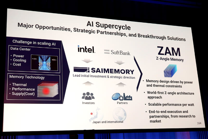
For SoftBank and SAIMEMORY, ZAM also fits into Japan’s broader semiconductor revival strategy. Japan has been investing heavily in advanced chip manufacturing, packaging, materials, and AI infrastructure, aiming to rebuild its position in the global semiconductor supply chain. Supporting ZAM through NEDO gives Japan another opportunity to participate in a potential future memory standard at a time when AI hardware demand continues to grow rapidly.
For Intel, the project could also reinforce its broader foundry and advanced packaging ambitions. ZAM is not just a memory technology story. It also connects to Intel’s larger strategy around heterogeneous integration, chiplet based design, EMIB, and future AI platforms. If Intel can combine advanced logic, advanced packaging, and next generation memory technology under one ecosystem, it could strengthen its position against rivals in the AI infrastructure market.
However, ZAM is still in development, and its commercial success is not guaranteed. The memory industry is highly demanding, and any HBM alternative must prove itself across performance, reliability, yield, manufacturing cost, customer adoption, supply chain readiness, and ecosystem support. HBM has a strong head start and is already deeply integrated into current AI accelerator roadmaps from major chip vendors. For ZAM to become a serious alternative, Intel and SAIMEMORY will need to demonstrate that it can scale beyond laboratory success and move into practical production.
That is why the NEDO support matters. Government backed funding and ecosystem coordination can help reduce development risk, bring partners together, and accelerate the long path from research to commercialization. In a market where memory bottlenecks are becoming one of the biggest challenges for AI and HPC growth, a successful ZAM rollout could have major implications.
Intel’s ZAM project now enters a 3.5 year development plan with stronger momentum and official backing from Japan. If successful, it could become one of the most important new memory architectures designed for the AI era, offering a low power, high density, wide bandwidth path beyond today’s HBM limitations.
The semiconductor industry is entering a phase where memory innovation may become just as important as compute innovation. ZAM is still early, but with Intel, SAIMEMORY, and NEDO now aligned, the project has become one to watch closely.
Will ZAM become a serious alternative to HBM for next generation AI systems, or will HBM remain the dominant memory standard for advanced accelerators?