
TSMC 2 nm Capacity Could Reach 110,000 Wafers per Month by Mid 2027
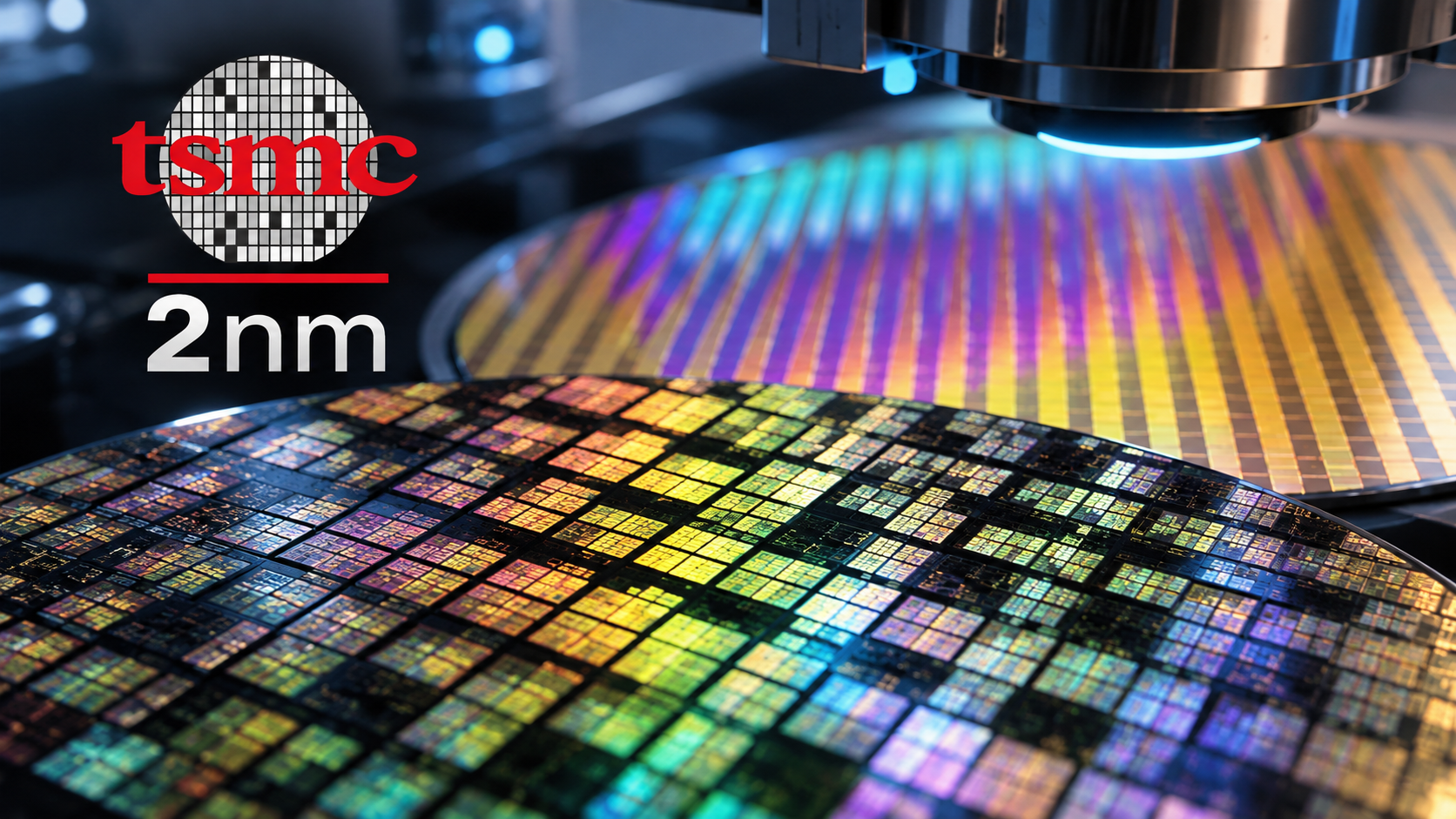
TSMC could expand its 2 nm production capacity to approximately 110,000 wafers per month by mid 2027 as demand for its newest manufacturing technologies continues accelerating across artificial intelligence, high performance computing, and premium consumer processors. The same expansion plan reportedly pushes 3 nm capacity beyond 210,000 wafers per month, showing that TSMC is scaling both leading process generations rather than immediately replacing N3 as N2 production increases.
According to Economic Daily News, supply chain sources say TSMC expects 2 nm monthly capacity to reach approximately 90,000 wafers by the end of 2026 before increasing to 110,000 by the middle of 2027. That represents an increase of roughly 22% in around 6 months. TSMC declined to comment on the market report and emphasized that capacity information should be based on official company announcements, meaning the 90,000 and 110,000 wafer figures remain supply chain estimates rather than formal TSMC guidance.
The same report indicates that 3 nm capacity will exceed 180,000 wafers per month by the end of 2026 before increasing beyond 210,000 by mid 2027. That represents growth of approximately 16.7% over the same period. While 2 nm is expanding faster in percentage terms, 3 nm still receives the larger absolute increase, adding around 30,000 monthly wafers compared with approximately 20,000 for 2 nm.
The longer term 3 nm expansion is even more substantial. Monthly N3 capacity reportedly stood between approximately 120,000 and 130,000 wafers at the end of 2025, which would put the platform near 70% capacity growth by the middle of 2027. Demand therefore remains strong even after N2 became TSMC's most advanced volume manufacturing platform.
That aligns with TSMC's own financial results. The company officially entered high volume N2 manufacturing during Q4 2025 at its Hsinchu and Kaohsiung facilities and has repeatedly described demand from smartphone, high performance computing, and artificial intelligence customers as strong. During Q2 2026, 2 nm already accounted for 3% of TSMC wafer revenue despite being in the early stages of its production ramp, while 3 nm accounted for 30%. TSMC expects the rapid N2 expansion to temporarily reduce gross margin by approximately 3 to 4 percentage points during 2H 2026 because of the costs associated with bringing a new process generation into large scale manufacturing.

TSMC is supporting the expansion with an enormous capital investment program. The company raised its 2026 capital expenditure forecast to between $60 billion and $64 billion, with approximately 70% to 80% directed toward advanced process technology. Another 10% to 20% is allocated across advanced packaging, testing, mask production, and related infrastructure, reflecting how manufacturing leading edge silicon increasingly requires simultaneous investment across the entire semiconductor production chain.
N2 is also developing into a much larger process family rather than remaining a single manufacturing node. N2P extends the original N2 platform with additional performance and efficiency improvements, while A16 introduces TSMC's Super Power Rail backside power delivery technology for high performance processors with dense power networks and complex signal routing. TSMC scheduled volume production of both technologies for 2H 2026.
The continued expansion of 3 nm is equally important. TSMC is adding N3 manufacturing capacity in Taiwan while its second Arizona fab is officially targeting volume production during 2H 2027. TSMC has also been optimizing capacity across process generations to extract more wafer output from existing facilities rather than relying exclusively on newly constructed fabs.
This simultaneous N2 and N3 expansion reflects how artificial intelligence has changed the traditional semiconductor transition cycle. A new process node would historically begin absorbing the most advanced products while demand for the previous generation gradually matured. Today, AI accelerators, server CPUs, smartphones, networking silicon, and custom processors are consuming multiple advanced nodes at the same time.
The manufacturing expansion also needs to be viewed alongside advanced packaging. TSMC could double CoWoS capacity to approximately 260,000 wafer equivalents per month by 2028, as NVIDIA, AMD, Broadcom, and major cloud companies compete for the packaging required to combine advanced compute dies with increasingly large HBM configurations.
Beyond N2, TSMC is already preparing its next major transistor generation. The company's official roadmap places A14 volume manufacturing in 2028, although construction progress in Taichung has created the possibility that A14 production could begin during 2H 2027. TSMC has not changed its official 2028 volume production target, making any earlier manufacturing schedule an accelerated possibility rather than confirmed guidance.
The headline number is 110,000 monthly 2 nm wafers, but the more interesting story is that TSMC is not choosing between N2 and N3. It is expanding both.
A move from 90,000 to 110,000 monthly N2 wafers represents approximately 22% growth in only 6 months, while N3 adds even more physical capacity during the same period. That suggests demand for leading edge silicon is broad enough to keep multiple generations operating at enormous scale simultaneously.
AI is a major reason. NVIDIA, AMD, custom cloud accelerators, server CPUs, mobile processors, and networking silicon do not all transition to the newest node at the same time. TSMC can therefore keep increasing N3 output while N2 ramps rapidly beside it.
The next bottleneck may increasingly sit outside the wafer fab. Producing more N2 and N3 dies matters only if advanced packaging, HBM, substrates, and testing capacity can scale quickly enough to turn those dies into complete products.
Do you think TSMC will face a larger capacity constraint from advanced process wafers or from CoWoS and HBM packaging as AI demand continues growing?
