
Samsung Pushes High NA EUV to 1nm as Cost and Technical Challenges Slow Adoption
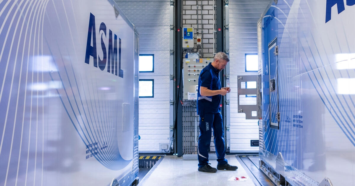
Samsung Electronics plans to introduce ASML High NA EUV lithography into volume manufacturing around its 1nm generation, delaying broader deployment of the technology after previously considering it for 2nm and 1.4nm processes. The decision places Samsung closer to TSMC's cautious strategy as both foundries attempt to extend existing 0.33 NA EUV equipment before committing heavily to ASML's significantly more expensive 0.55 NA platform.
According to ZDNet Korea, Samsung semiconductor lithography specialist ChangMin Park revealed the updated roadmap during the 2026 Next Generation Lithography + Patterning Conference in Suwon, South Korea. Samsung had originally hoped to introduce High NA EUV during production of its 2nm and 1.4nm technologies, but Park said the ecosystem still requires additional technical refinement.
"We wanted to apply High NA EUV to 2nm and 1.4nm mass production, but technical improvements are still needed."
— Quote by: ChangMin Park
Samsung currently expects High NA EUV to become necessary beginning around its A10 generation, corresponding to the 1nm class. The company is working with equipment and materials partners to prepare the technology, with volume implementation potentially beginning around 2030. Samsung currently plans SF1.4 production for 2029, followed by SF1.4+ and its 1nm generation around 2030.
High NA EUV increases numerical aperture from 0.33 on current EUV systems to 0.55. According to ASML, its EXE platform can achieve an 8nm critical dimension, allowing features around 1.7 times smaller and potentially 2.9 times greater transistor density compared with its existing NXE platform. The increased resolution can also replace some complex multiple patterning steps with a single exposure, potentially reducing manufacturing complexity and defect opportunities.
The technological advantage comes with a substantial economic barrier. ASML High NA systems can cost as much as approximately $400 million each, and TSMC has already indicated that the equipment remains too expensive to justify for its immediate manufacturing roadmap. The Taiwanese foundry is therefore continuing to optimize conventional EUV and multiple patterning rather than introducing High NA across its upcoming processes.
That strategy is already visible in TSMC's A14 manufacturing plans. The company is preparing its 1.4nm class technology without depending on High NA EUV, betting that established lithography equipment and increasingly sophisticated patterning techniques can remain economically competitive for another generation.
Intel is taking a substantially different approach. In July, ASML confirmed that Intel Foundry had entered high volume manufacturing using High NA EUV on selected Intel 18A layers for a subset of Core Ultra Series 3 Panther Lake processors. Intel became the first chipmaker to ship high volume logic products using the technology, giving ASML an important production validation even as Samsung and TSMC remain more conservative about widespread adoption.
Samsung does not intend to abandon High NA. Park explained that conventional 0.33 NA EUV multiple patterning is expected to remain the mainstream approach through its 1.4nm and early 1nm generation, while High NA should become increasingly important for subsequent technologies. The transition may therefore happen gradually, with manufacturers using different lithography approaches depending on the layer, cost, yield, and technical requirements of each process.
High NA EUV is no longer a question of whether the semiconductor industry can make it work. Intel has already demonstrated production silicon using the technology. The larger question is when its manufacturing advantages justify a machine costing as much as $400 million.
Samsung and TSMC appear willing to extract considerably more life from conventional EUV through multiple patterning, while Intel is accepting the earlier cost and integration challenge to gain manufacturing experience ahead of future nodes. If High NA eventually becomes essential below 1nm, Intel could benefit from that head start. If conventional EUV remains economically competitive longer than expected, Samsung and TSMC may instead benefit from delaying one of the semiconductor industry's most expensive equipment transitions.
Will Intel's early adoption of High NA EUV become a manufacturing advantage, or are Samsung and TSMC making the smarter decision by waiting until the technology becomes more mature and economical?
