
NVIDIA Custom HBM Could Bring Samsung and TSMC Together on 3 nm Base Dies
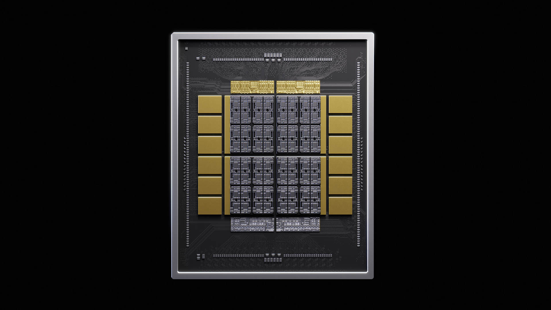
NVIDIA is reportedly bringing semiconductor rivals Samsung and TSMC together to manufacture custom High Bandwidth Memory (HBM), with Samsung agreeing to use TSMC's advanced 3 nm process for the logic base die of NVIDIA's upcoming NVHBM architecture. The arrangement would mark a significant departure from Samsung's traditional manufacturing strategy, which relies on producing both DRAM core dies and logic base dies through its own semiconductor facilities.
According to an October 18 report from Seoul Economic Daily, citing industry sources, NVIDIA has requested that Samsung, SK hynix, and Micron standardize NVHBM production using TSMC's 3 nm technology for the base die and sixth generation 1c DRAM for the memory dies. Samsung reportedly accepted the requirements following an internal evaluation, allowing NVIDIA to pursue consistent memory performance across multiple suppliers while reducing the complexity of product qualification. Neither NVIDIA, Samsung, nor TSMC has publicly confirmed the manufacturing arrangement.
The development builds on NVIDIA's NVHBM architecture, introduced in August 2026, which relocates the memory controller from the GPU or XPU directly into the HBM base die. This approach frees additional silicon area for computing resources while optimizing communication between the accelerator and memory. NVIDIA claims the architecture can deliver up to 30% more memory bandwidth, 15% lower HBM power consumption, and 25% more available XPU compute die area compared with conventional HBM4E. These remain manufacturer performance claims rather than independently verified commercial results.
Standard HBM4E vs NVIDIA NVHBM
| Feature | Standard HBM4E | NVIDIA NVHBM |
|---|---|---|
| Memory controller | Located on GPU or XPU | Integrated into HBM base die |
| Base die manufacturing | Varies by supplier | TSMC 3 nm reportedly requested |
| DRAM manufacturing | Supplier dependent | Sixth generation 1c requested |
| Memory bandwidth | Baseline | Up to 30% higher, NVIDIA claim |
| HBM power consumption | Baseline | Up to 15% lower, NVIDIA claim |
| Supplier qualification | Vendor specific validation | Standardized NVIDIA architecture |
The 3 nm manufacturing arrangement and 1c DRAM requirements are based on industry reporting. Performance improvements are NVIDIA projections relative to standard HBM4E.
Samsung currently manufactures its standard HBM4 and HBM4E base dies using its own 4 nm process, maintaining control over memory manufacturing and packaging. Adopting TSMC's 3 nm technology for NVHBM would introduce an external foundry into that process, although Samsung reportedly intends to retain its existing manufacturing approach for standard HBM and other customized products.
The company is also reportedly evaluating production of NVHBM base dies using its own 2 nm process as a potential alternative if TSMC encounters capacity limitations. This reflects growing demand for advanced logic manufacturing as HBM base dies become increasingly sophisticated and expensive, a trend already influencing NVIDIA's strategy for controlling more of the technology and economics behind AI memory.
For NVIDIA, standardizing the base die across multiple memory suppliers could improve supply flexibility while simplifying integration into future AI accelerators. However, the arrangement could also increase dependence on TSMC's advanced manufacturing capacity. Production volumes, commercial availability, and pricing for NVHBM have not been disclosed.
NVIDIA's reported decision to standardize NVHBM manufacturing through TSMC could reshape relationships within the advanced memory industry. By controlling the memory controller architecture and specifying a common manufacturing process, NVIDIA gains greater influence over a critical component of future AI accelerators.
For Samsung, working with a direct foundry competitor represents a strategic compromise, but it could also help secure participation in NVIDIA's growing custom memory ecosystem. The challenge will be balancing manufacturing independence against customer requirements and production capacity.
The broader implications extend beyond AI performance. As advanced base dies require increasingly expensive logic processes, HBM manufacturing costs and foundry capacity could become just as important as DRAM production itself. The arrangement may improve supply flexibility, but it does not guarantee lower memory prices or faster capacity expansion.
Could NVIDIA's standardized NVHBM architecture reduce the influence of Samsung, SK hynix, and Micron over AI memory development, or will advanced DRAM manufacturing remain their strongest competitive advantage?
