
Intel and Partners Showcase Z Angle Memory Prototype as a Potential Path Beyond HBM Thermal Limits

Intel and a group of partners are positioning a new stacked memory concept called Z Angle Memory, also referred to as ZAM, as a way to address the thermal density and compute era constraints that continue to tighten around today’s high bandwidth memory approach. The first widely reported public overview of the project appeared at Intel Connection Japan 2026, where Japanese outlet PC Watch reported on the initial presentation and prototype level messaging tied to the effort.
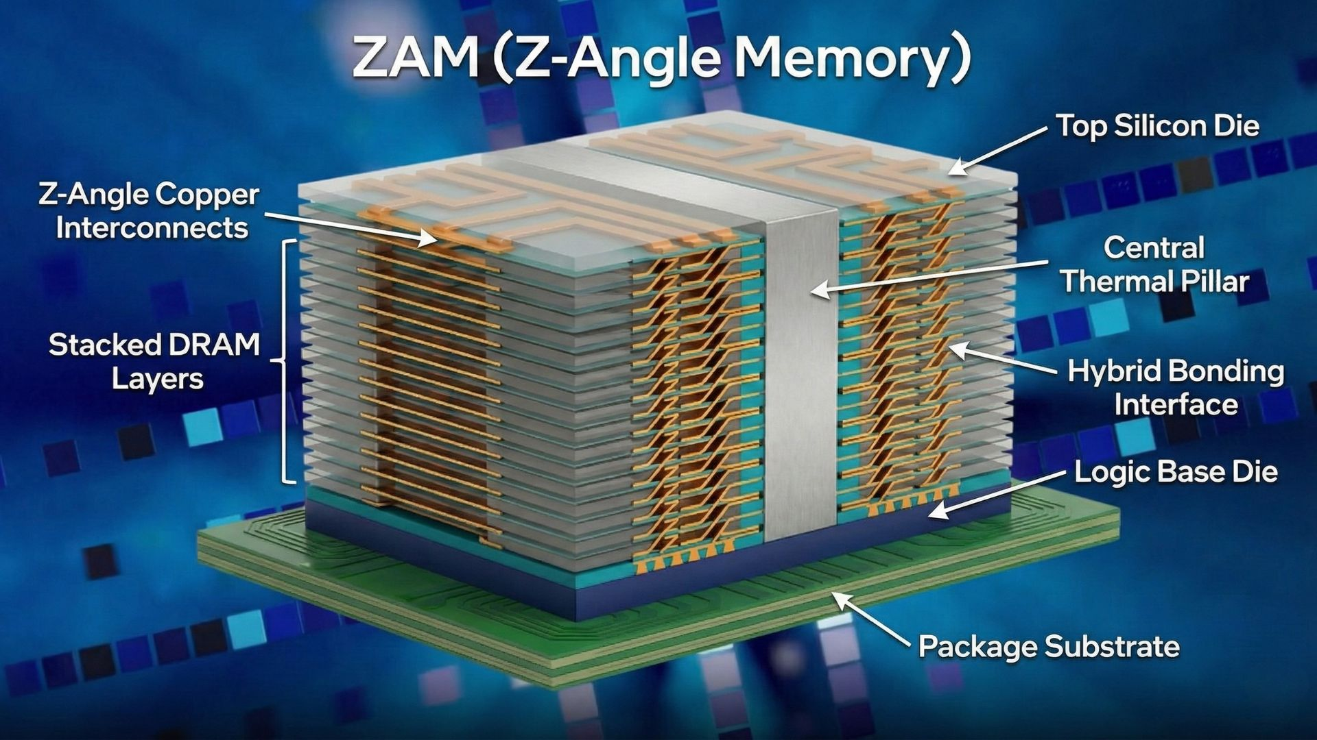
The core pitch is architectural. Instead of relying purely on straight vertical pathways through the stack, the Z Angle approach routes interconnects diagonally across dies in a staggered topology, with Intel and its partners arguing this can distribute heat more effectively and reduce hotspots that become performance limiting in dense memory stacks. In the AI infrastructure era, where memory bandwidth, capacity, and thermals often gate system level scaling, the project is being framed as a direct attempt to create a credible alternative lane to HBM, not a niche experiment.
The Intel Connection Japan 2026 unveiling was notable for who showed up. The event featured Intel Fellow Joshua Fryman, who is also the CTO of Intel Government Technologies, alongside Intel Japan leadership, a clear indicator that Intel views the program as more than a lightweight research collaboration. At the same time, early materials suggest Intel’s role centers on initial investment and strategic decision making, while the partner ecosystem drives the memory technology ramp, which fits Intel’s current posture of influencing adjacent platform pillars without re entering commodity DRAM manufacturing directly.
Initial claims being circulated around ZAM’s potential upside are aggressive and aimed squarely at the AI data center value proposition. Early talking points include 40 to 50% lower power consumption, simplified manufacturing via the Z angle interconnect approach, and higher storage per chip reaching up to 512GB. Those numbers should be treated as aspirational until there is broader independent validation and yield clarity, but the direction is consistent with what the market wants most: more capacity and bandwidth per footprint without thermal runaway.

For the broader industry, the most important strategic implication is not that HBM is suddenly at risk overnight, but that serious players are investing in a post HBM narrative because current scaling economics are colliding with packaging complexity, thermal density, and power budgets. If ZAM progresses from prototype messaging into a repeatable manufacturing path with healthy yields, it could become a meaningful second option for AI accelerators and advanced compute platforms. If it does not, the effort still reinforces a reality gamers already feel in their wallets: the highest margin AI memory tiers will keep pulling engineering focus and capacity away from consumer friendly cost curves.
Do you think alternative stacked memory designs like Z Angle Memory can realistically break HBM dominance, or will yield and packaging complexity keep HBM as the only viable choice for years?