
IBM Opens New Office Near Rapidus 2nm Fab as Japan Targets Mass Production in 2027
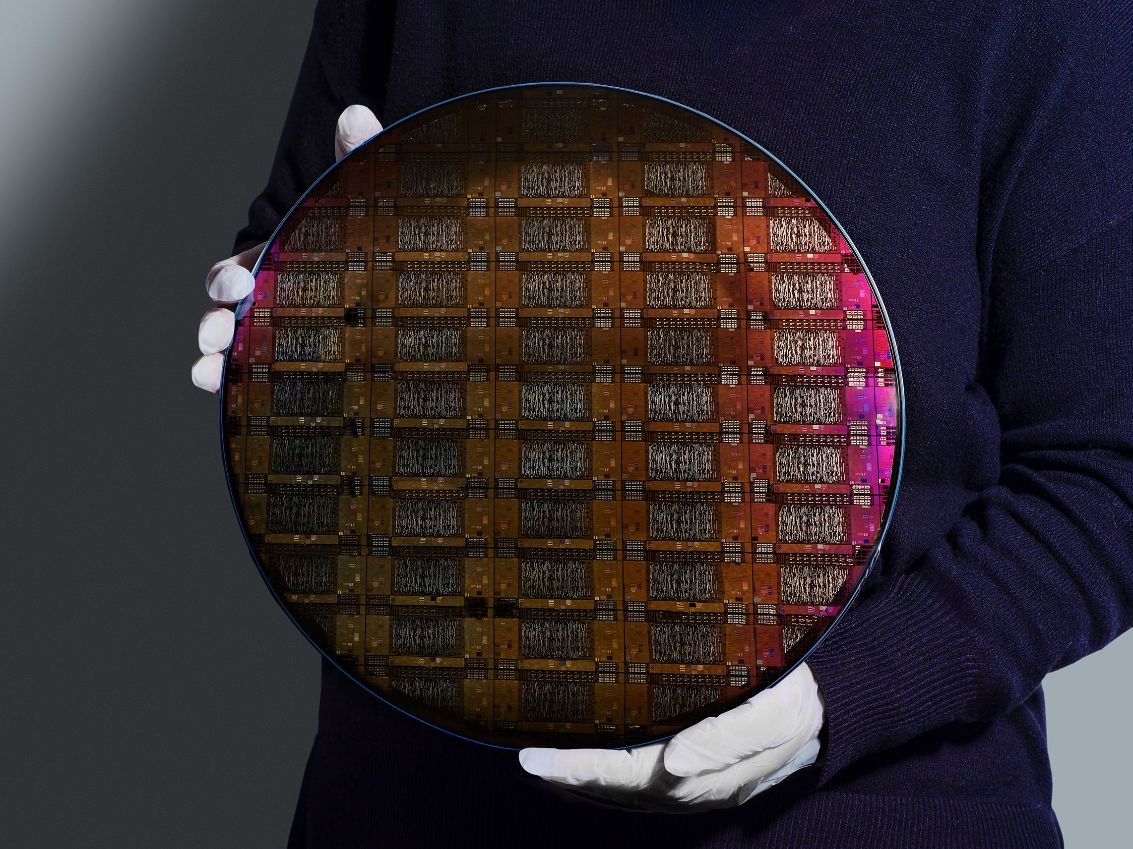
IBM has officially opened a new office in Chitose, Hokkaido, strengthening its partnership with Japanese semiconductor manufacturer Rapidus as the country accelerates efforts to establish domestic 2nm chip production. The expansion brings IBM closer to Rapidus' IIM 1 fabrication facility, where the company aims to begin commercial manufacturing of advanced processors in the second half of fiscal 2027, potentially introducing another competitor to TSMC, Samsung and Intel in the advanced semiconductor market.
According to IBM Japan's official announcement, published on October 26, the new facility will strengthen support for semiconductor customers, including Rapidus, while expanding cooperation with local businesses, research organizations and government institutions. The office is located in Chitose's Chiyoda district, near the semiconductor manufacturing ecosystem developing around Rapidus' factory.
The expansion builds upon the strategic partnership established in December 2022, when both companies agreed to jointly develop IBM's 2nm semiconductor technology for manufacturing in Japan. Since then, Rapidus engineers have worked alongside IBM researchers at the Albany NanoTech Complex in New York, transferring advanced transistor manufacturing expertise to Japan.
The collaboration focuses on Gate All Around (GAA) nanosheet transistors, which replace conventional FinFET structures with vertically stacked silicon channels surrounded by gate electrodes. This design offers improved electrostatic control, potentially reducing leakage current while supporting higher performance and better power efficiency.
IBM originally demonstrated its 2nm nanosheet technology in 2021, projecting up to 45% higher performance or 75% lower energy consumption compared with 7nm technology under different operating conditions. These figures represent IBM's early research projections rather than verified performance results from Rapidus' commercial manufacturing process.
Rapidus has already made measurable progress at its IIM 1 semiconductor facility, beginning pilot production in April 2025 and successfully demonstrating working 2nm GAA transistors in July of the same year. The facility also installed Japan's first EUV lithography system intended for advanced volume production, supplied by ASML.

In April 2026, Rapidus expanded its local development infrastructure with a dedicated analysis center and Rapidus Chiplet Solutions, supporting electrical characterization, reliability testing and advanced packaging development. IBM has also contributed its SiView Standard manufacturing execution system, which supports equipment integration, production automation and process monitoring at IIM 1.
Japan's efforts to establish a competitive domestic foundry have attracted substantial government support, with Rapidus securing ¥267.6 billion in additional funding in February 2026. However, successfully manufacturing prototype transistors remains different from producing commercially viable chips at scale.
As highlighted by Rapidus' reported production expansion plans, the company is pursuing significant capacity growth through 2028. Achieving competitive yields, securing customers and controlling manufacturing costs will be essential to that expansion.
IBM's presence in Chitose strengthens the local technical and business support infrastructure, but the company has not disclosed additional manufacturing commitments, staffing levels or a revised production schedule. Rapidus continues targeting the second half of fiscal 2027 for mass production, with its commercial readiness still dependent on manufacturing development and financial execution.
IBM's expansion into Chitose represents an important step in Japan's attempt to rebuild its position in advanced semiconductor manufacturing. Rather than relying exclusively on overseas research partnerships, Rapidus is developing a domestic ecosystem combining fabrication, testing, packaging and technical expertise.
The biggest challenge, however, is not developing a working 2nm transistor. TSMC, Samsung and Intel already possess extensive manufacturing experience, established customer relationships and production infrastructure that Rapidus must compete against.
For AI accelerators, server processors and future computing hardware, an additional advanced foundry could provide valuable supply chain diversification. Rapidus' strategy of targeting shorter manufacturing turnaround times may also appeal to specialized AI chip designers and smaller semiconductor companies.
IBM's local presence should help strengthen that foundation, but the real measure of success will be whether Rapidus can deliver commercially competitive yields and consistent production volumes. Japan's 2nm ambitions are progressing, although establishing a viable alternative to existing foundry leaders will require more than meeting the initial 2027 production target.
Do you think IBM and Rapidus can establish Japan as a serious competitor to TSMC, Samsung and Intel in advanced semiconductor manufacturing, or will production yields and manufacturing costs remain their biggest obstacles?
