
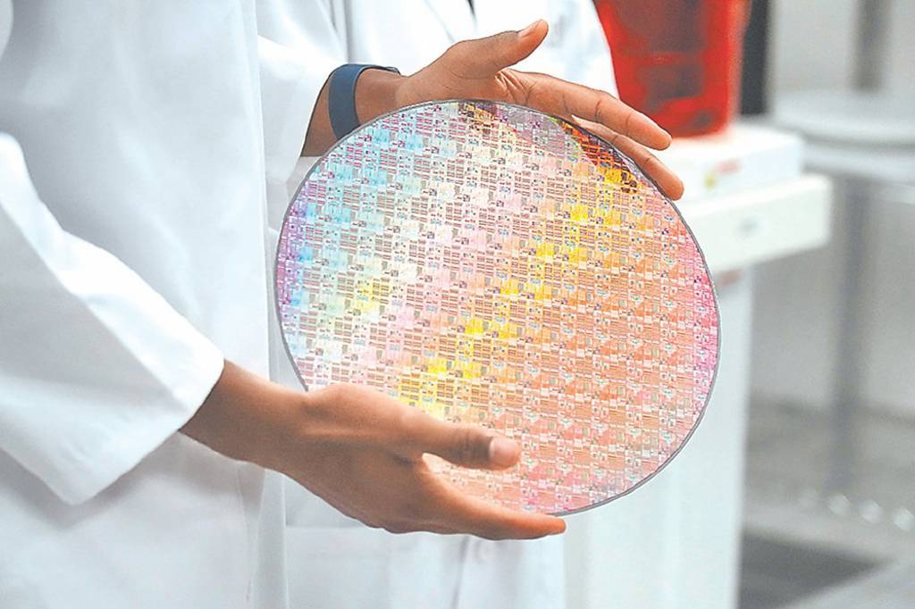
Rapidus Accelerates 2nm Push and Targets 60,000 WPM by 2028, Setting Up a Japan Foundry Face Off with TSMC

Rapidus is turning its 2nm ambition into a clear scale plan, and the latest reporting signals that Japan’s most aggressive native foundry project is now mapping out a dramatic production ramp through 2028. In a market where AI demand is compressing timelines and concentrating orders around a handful of leading edge fabs, Rapidus is positioning itself as a credible alternative on the most valuable frontier node, and it is doing it on home turf where TSMC is also expanding its footprint.
According to a new report cited by Yahoo Japan, Rapidus plans to begin full scale production by 2028 and scale capacity to 60,000 wafers per month by that year. The same report describes a stepwise ramp, reaching around 6,000 WPM by 2027 and then multiplying output by roughly 4 times the following year as the company moves into higher volume operations.
One of the most important near term signals is that Rapidus has recently indicated PDK kits will be available to customers in 2026. That matters because a process can only become commercially real once partners can begin practical design enablement, validate libraries, and de risk tapeout planning. In foundry business terms, PDK availability is a gating milestone that shifts the conversation from aspiration to execution readiness, especially for customers that need to lock design rules early to hit 2027 and 2028 product windows.
On the technology side, details remain limited, but the node is expected to be branded as 2HP. A prior report referenced logic density at 237.31 MTr per mm², positioned as comparable to TSMC N2 in density terms. Rapidus is also planning to employ single wafer front end processing, a differentiated manufacturing approach that emphasizes making adjustments at limited production volume, then scaling improvements as confidence grows. This strategy reads like a deliberate attempt to optimize learning cycles and yield ramp efficiency, but the real industry verdict will come down to high volume manufacturing consistency, defect control, and cycle time once output begins scaling rapidly.
The competitive tension is hard to miss. While Rapidus is building Japan’s leading edge narrative, TSMC is simultaneously scaling up in Japan, with its Kumamoto expansion reportedly pivoting toward 3nm for the second fab. Even if TSMC’s move is primarily about addressing global demand and diversifying supply chains, the timing creates an unavoidable comparison in the market. Japan is no longer just a manufacturing geography in the background. It is increasingly becoming an arena where leading edge capacity, ecosystem investment, and national industrial strategy collide.
For the industry, the forward looking question is not whether there is demand for leading edge wafers. Demand is already there. The question is whether Rapidus can translate its roadmap into stable high volume output on schedule, and whether customers will see enough value in a Japan based 2nm option to diversify away from the established giants. If Rapidus hits its stated ramp targets and gets real tapeouts flowing after PDK release, the next 24 months will define whether this becomes a true foundry showdown or a long ramp toward niche specialization.
If Rapidus delivers 2nm on schedule, do you see it becoming a serious second source for leading edge silicon in Japan, or will most customers still default to TSMC for risk control?