
CXMT Secures Early Access to China’s Homegrown DUV Machines as Its 3D DRAM Strategy Accelerates
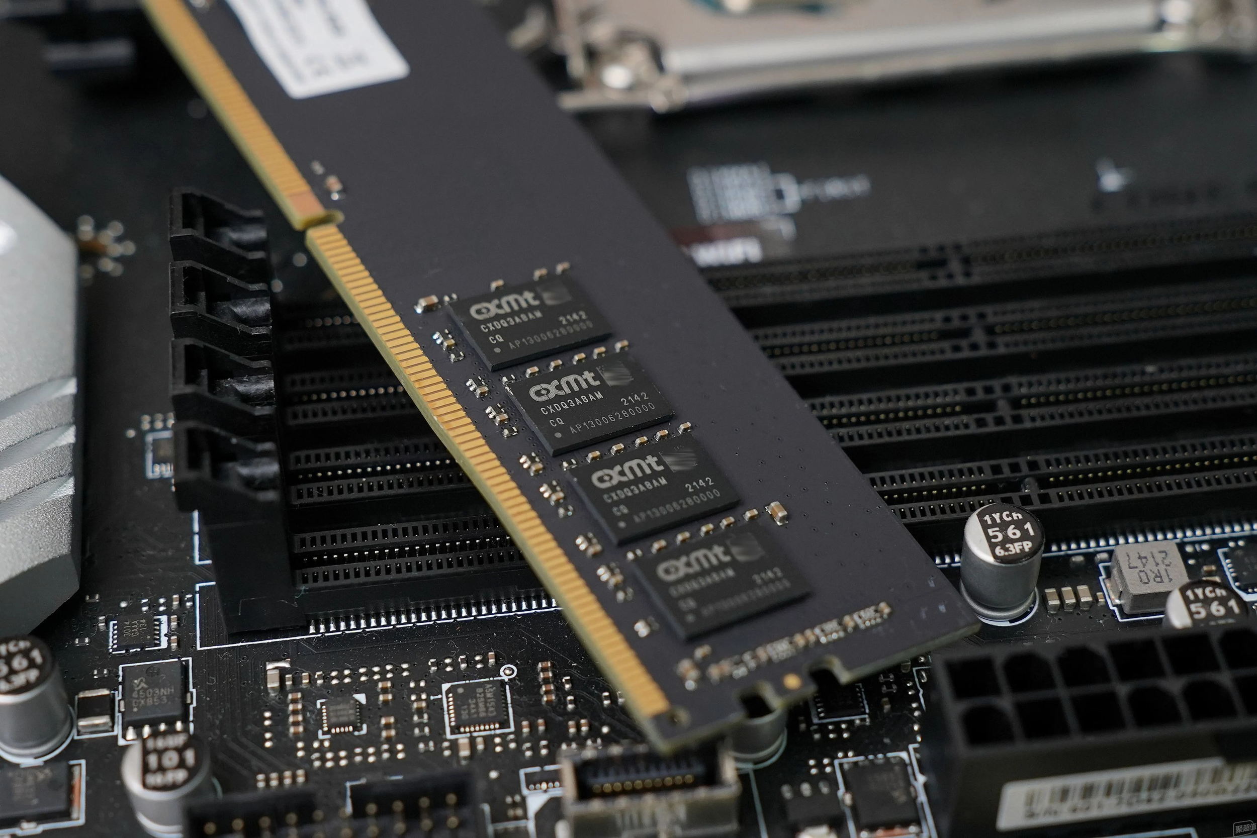
CXMT is reportedly among the first Chinese semiconductor manufacturers scheduled to receive domestically produced immersion Deep Ultraviolet lithography systems, giving the memory company a potential alternative to restricted Western manufacturing equipment as it expands DRAM production.
According to Reuters, Shanghai Aishengna Electronic Technology Group has started producing homegrown immersion DUV machines after incorporating engineering teams from Chinese lithography developers, including Shanghai Micro Electronics Equipment and Yuliangsheng. The state owned company reportedly plans to manufacture approximately 5 machines during 2026 and around 20 during 2027.
The first systems are expected to reach SMIC, Hua Hong Semiconductor, and CXMT before the end of 2026. However, the machines still require further testing and remain considerably behind competing systems from ASML in performance and manufacturing maturity. They should therefore be viewed as an early domestic alternative rather than an immediate replacement for the Dutch company’s established lithography portfolio.
Immersion DUV technology uses 193 nm ultraviolet light and a layer of water between the projection lens and silicon wafer to print smaller circuit patterns. A modern system can produce approximately 28 nm class features through a single exposure, while manufacturers can use repeated exposures and multiple patterning to produce substantially smaller structures. This approach increases production complexity, cost, overlay risk, and the possibility of yield losses compared with processes using Extreme Ultraviolet lithography.
For CXMT, access to domestic lithography equipment could become strategically important. The company remains dependent on foreign DUV systems, while Samsung, SK hynix, and Micron use more advanced EUV equipment for selected DRAM layers. China has been blocked from purchasing ASML’s EUV machines since the Netherlands began withholding export licenses in 2019.
The domestic machines could also reduce CXMT’s exposure to the proposed MATCH Act. Introduced in the United States Congress in April 2026, the legislation seeks to align semiconductor equipment restrictions across the United States, Japan, the Netherlands, and other allied countries. It would also target servicing and continued support for selected tools already operating inside China.
However, describing China’s DUV development as completely neutralizing the MATCH Act would be premature. Initial production remains extremely limited, and domestic machines have not yet demonstrated the throughput, accuracy, reliability, or manufacturing yields required to replace ASML equipment at scale. Successful deployment would instead give Chinese manufacturers an additional supply path if foreign equipment sales and servicing become more restricted.
The timing is favorable for CXMT, which completed its Shanghai market debut on July 27, 2026. Shares closed 466% above their offering price after the company raised $8.6 billion through the largest mainland Chinese semiconductor offering on record. CXMT finished its first trading day with a market capitalization of approximately $487.73 billion, although only 6.73% of its enlarged share capital was freely tradable, contributing to extreme price volatility.
The capital will support CXMT’s aggressive manufacturing expansion. The company is building new fabrication facilities in Shanghai and Hefei and is reportedly discussing another site with regional authorities. If completed as planned, the projects could increase its production capacity to more than 600,000 wafers per month and potentially place CXMT ahead of Micron in manufacturing volume by 2030.
Domestic DUV access could also support CXMT’s longer term interest in 3D DRAM. Patent filings associated with the company describe vertically structured memory using Gate All Around wordlines, horizontal bitlines, and horizontally arranged capacitors. Other reports suggest CXMT is investigating wafer to wafer hybrid bonding, where the memory array and control logic are manufactured separately before being bonded together.
This approach would not remove the need for precise lithography, but it could allow CXMT to improve density by building upward rather than relying exclusively on increasingly aggressive horizontal scaling. Domestic DUV systems, multiple patterning, design technology co optimization, and hybrid bonding could therefore become complementary parts of its attempt to progress without access to EUV.
China producing immersion DUV systems is a meaningful semiconductor milestone, but manufacturing 5 machines is fundamentally different from operating a mature lithography supply chain. CXMT will need consistent overlay accuracy, high wafer throughput, dependable servicing, and competitive yields before domestic equipment can replace foreign systems across advanced DRAM production.
The more important development is the direction of travel. CXMT now has substantial capital, expanding capacity, growing pricing power, and priority access to strategic domestic equipment. Combining those resources with 3D DRAM and hybrid bonding research could reduce the company’s dependence on the same scaling roadmap followed by Samsung, SK hynix, and Micron.
China has not eliminated its lithography gap, but it is beginning to build enough domestic alternatives to make future export restrictions less decisive.
Could domestic DUV and 3D DRAM eventually allow CXMT to compete without access to EUV equipment?
