
China Develops DUV GAA Transistors, but Full Process Still Faces 5 nm Class Density Limits
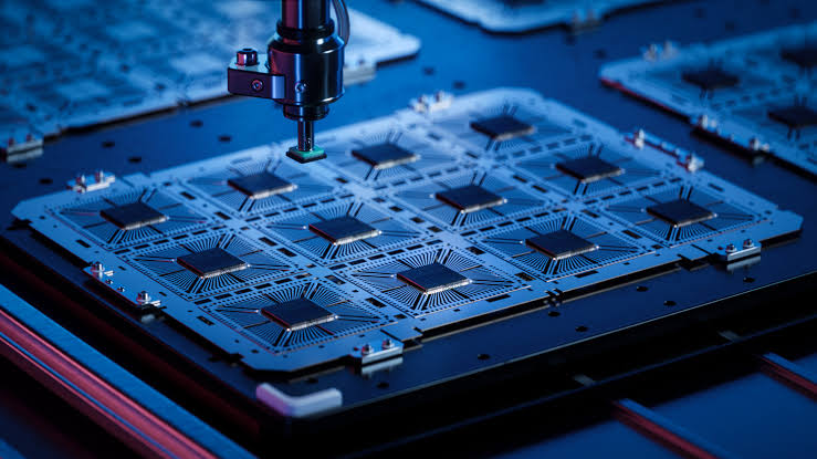
China has demonstrated a stacked nanosheet Gate All Around CMOS process built around DUV lithography, presenting a possible research route toward transistor structures intended for nodes below 3 nm without relying on EUV for every critical layer. The work is technically notable, but it should not be interpreted as a complete 3 nm class manufacturing process built with DUV.
Ye Tianchun of the Institute of Microelectronics at the Chinese Academy of Sciences disclosed the work during ICDIA 2026. According to his presentation, the institute established an early process integration flow for stacked nanosheet GAA CMOS under DUV lithography and completed CMOS device development. Process optimization produced an on to off current ratio above 5 × 10⁵, with Ye describing the work as a potential GAA research path for processes below 3 nm.
That figure needs context. An Ion/Ioff ratio above 500,000 suggests strong control over leakage current, an area where GAA structures can offer advantages over older transistor designs. It does not establish equivalence with commercial 3 nm processes from TSMC or Samsung. Node competitiveness also depends on drive current, power, density, interconnects, yield, design libraries, manufacturability, and cost.
The Chinese Academy of Sciences has been researching GAA technology for several years. Its Institute of Microelectronics previously demonstrated FishboneFET and TreeFET CMOS devices and later reported GAA devices reaching 965 μA/μm on state current with parasitic source and drain resistance reduced to 100 Ω. The latest DUV work appears to build on that broader device research rather than representing an isolated result.
But once FEOL fin pitch can be relax by GAA, then even SMIC poly pitch is constrained by MEOL, the cell height can be shrink by reducing the M0 track number from 5 (N+3) to 4.
— aog T (@Taog_1575) September 17, 2026
So G57H198 or G54H198 (density 137.8, N5 class) could be achieved:https://t.co/GyptbG09it https://t.co/wlDQEzOBr9
The next challenge is integrating those transistors into dense logic.
Front End Of Line manufacturing creates the transistor structures themselves. Middle End Of Line forms the contacts connecting those devices, while Back End Of Line creates the metal wiring network above them. Improvements at the transistor level do not necessarily translate directly into equivalent scaling across the contact and interconnect layers.
External semiconductor analysis has suggested that those constraints could significantly limit overall density. One proposed layout using a reduced 4 track M0 cell was estimated at around 137.8 million transistors per mm², a density more comparable with estimates associated with TSMC N5 than current 3 nm processes. This is a modeled projection rather than a measured result from a production process, so it should be treated as an indication of the possible limitation rather than a confirmed density figure.
DUV itself can still be pushed to smaller dimensions through multiple patterning, but doing so generally requires additional masks and process steps while increasing overlay requirements. How practical such an approach becomes at very advanced geometries depends heavily on yield, cost, and process control, none of which have been demonstrated for this research flow.
China is also working to expand its domestic lithography capabilities.Shanghai Aishengna has begun China's domestic immersion DUV push, with initial systems expected to reach Chinese fabs during 2026 and 2027. Restricted access to commercial EUV equipment gives Chinese researchers a strong incentive to investigate alternative transistor structures and more aggressive uses of DUV.
The most interesting part of this work is not a claim that China has reproduced a commercial 3 nm process without EUV. The available information does not support that conclusion.
What the research does show is continued progress on GAA transistor structures under a DUV based process flow. That could become useful if similar device characteristics can eventually be combined with competitive contacts, interconnects, density, yields, and manufacturing economics.
How much this approach can narrow the gap with leading commercial nodes remains unclear. The reported transistor results address one part of the manufacturing problem, while several other parts of a complete advanced process have not yet been demonstrated publicly.
For now, it is better viewed as evidence of progress in advanced transistor research rather than proof of a production ready alternative to established 3 nm technologies.
How far do you think advanced transistor structures and 3D integration can extend DUV manufacturing before EUV becomes unavoidable?
