
AMD Versal Premium Gen 2 Packs 32 GB LPDDR5X Into a Smaller PCIe 6.0 SoC

AMD has introduced the Versal Premium Gen 2 Memory on Package family, a new collection of adaptive system on chips that integrates up to 32 GB of LPDDR5X directly inside the processor package. The design delivers up to 288 GB/s of projected memory bandwidth while reducing the required board area by more than 60% compared with a similar Versal Premium Gen 2 configuration using external LPDDR5X memory.
The announcement expands the existing Versal Premium Gen 2 platform, which was originally introduced in 2024 with support for PCIe 6.0, CXL 3.1, DDR5, LPDDR5X, and transceiver speeds reaching 128 Gb/s. The new Memory on Package models retain those connectivity capabilities while eliminating the need to place and route the main LPDDR5X memory devices separately across the system board.
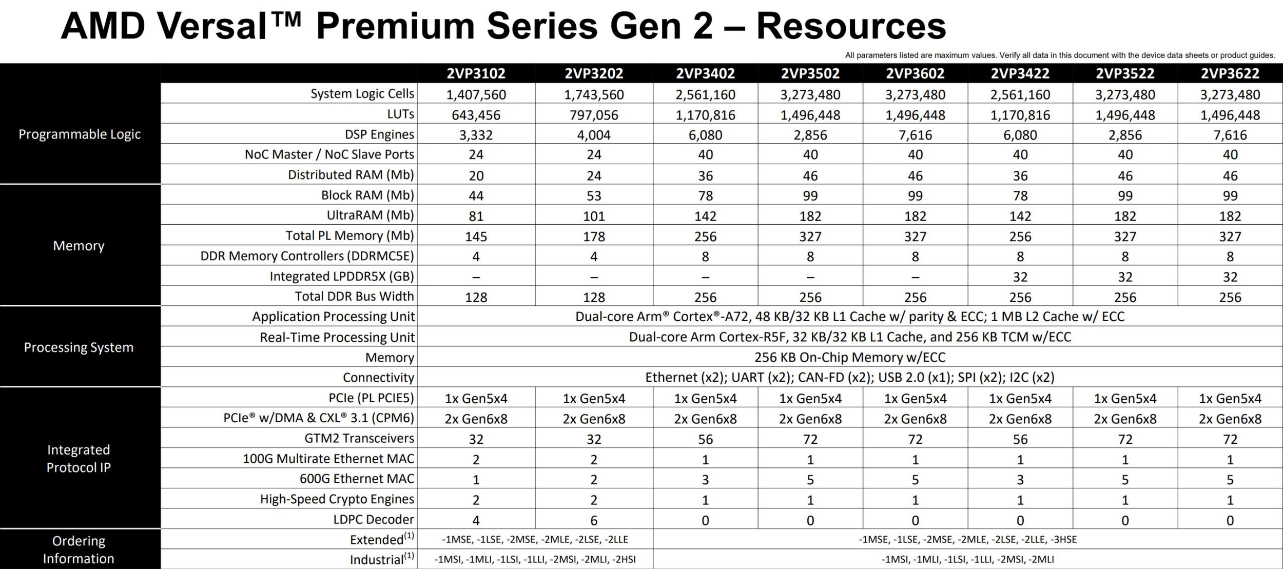
AMD is offering 3 initial devices named 2VP3422, 2VP3522, and 2VP3622. Every model integrates 32 GB of LPDDR5X through 8 memory controllers with 32 bit interfaces, while their programmable logic, DSP resources, and transceiver configurations differ according to the intended application.
| Device Name | 2VP3422 | 2VP3522 | 2VP3622 |
|---|---|---|---|
| System Logic Cells (K) | 2,561 | 3,273 | 3,273 |
| CLB LUTs (K) | 1,172 | 1,496 | 1,496 |
| Total RAM (Mb)* | 256 | 327 | 327 |
| Integrated LPDDR5X Capacity / Controllers | 32 GB / Eight x32b | 32 GB / Eight x32b | 32 GB / Eight x32b |
| DSP Engines | 6,080 | 2,512 | 7,616 |
| PCIe w/ DMA & CXL 3.1 (CPM6) | 2x Gen6x8 | 2x Gen6x8 | 2x Gen6x8 |
| Max. I/O (XP5IO/MIO) | 194 / 78 | 194 / 78 | 194 / 78 |
| GTM2 Transceivers | 56 | 72 | 72 |
The integrated memory operates at speeds reaching 9000 Mb/s and provides up to 288 GB/s of projected bandwidth. AMD says this represents approximately 5% more bandwidth than an equivalent design using external LPDDR5X, which can reach around 270 GB/s. The larger advantage comes from integration, since engineers no longer need to design, simulate, route, and validate several extremely fast memory channels across the printed circuit board.
“Memory on Package removes that tradeoff.”
— Sumit Shah, Head of Product Management and Marketing at AMD
AMD says the prevalidated memory interface can shorten development cycles, reduce signal integrity and power integrity work, lower the possibility of expensive board revisions, and allow customers to reuse familiar Vivado and Vitis development environments. Existing designs targeting standard Versal Premium Gen 2 devices should also be able to transition to the Memory on Package versions without rebuilding the complete software and programmable logic workflow.
The reduced board area is intended to enable compact systems that would be difficult to build around external high speed memory. AMD specifically identifies EDSFF cards, PCIe accelerators, PXI test equipment, professional video systems, telecommunications hardware, and 3U VPX platforms used for aerospace, defense, and secure communications.
Every announced model includes 2 PCIe 6.0 x8 controllers with direct memory access and CXL 3.1 support in hard IP. PCIe 6.0 operates at 64 GT/s per lane, while CXL allows memory coherent communication between the adaptive SoC, host processors, and external memory expansion devices. AMD is positioning the chips for use alongside EPYC processors in systems that need to move large amounts of data between compute, storage, networking, and accelerator resources.

Security features include PCIe Integrity and Data Encryption for protecting information moving across the physical link, encryption inside the dedicated DDR memory controllers, inline error correction, and hard 400G cryptography engines. These functions allow system designers to protect data without consuming a large amount of programmable logic that could otherwise be used for application acceleration.
Versal Premium Gen 2 Memory on Package devices are rated for industrial operation between minus 40 degrees Celsius and 110 degrees Celsius. AMD is also promising more than 15 years of lifecycle support, targeting equipment that must remain available and serviceable long after ordinary consumer or data center hardware has been replaced.
AMD specifically says LPDDR5X helps customers reduce their dependence on the shorter, data center driven product cycles associated with HBM. This does not mean the new devices outperform the existing Versal HBM family. Versal HBM products already integrate up to 32 GB of HBM2E and provide as much as 819 GB/s of bandwidth, nearly 3 times the 288 GB/s projected for the LPDDR5X design.
The new family therefore represents an alternative for applications prioritizing board space, availability, power, cost, and long lifecycle support rather than the highest possible memory bandwidth. Current HBM and wider DRAM shortages make that flexibility commercially valuable, but AMD has not stated that supply constraints were the direct reason for creating the product. The wider industry is also adopting LPDDR memory for systems beyond smartphones and notebooks. NVIDIA is using large quantities of LPDDR5X around its Vera CPU platform, while JEDEC is preparing LPDDR6 based SOCAMM2 memory for future artificial intelligence servers.

The frequently referenced 10x compute improvement does not specifically describe the new Versal Premium Gen 2 Memory on Package models. AMD uses that claim for selected Versal AI Edge Gen 2 and Versal Prime Gen 2 devices equipped with substantially upgraded Arm processing systems, compared with earlier Versal or Zynq products. AMD’s published specifications for the Premium Gen 2 Memory on Package family focus instead on programmable logic, DSP engines, memory bandwidth, connectivity, security, and compact system integration.
AMD Versal Premium Gen 2 Memory on Package devices are scheduled to begin sampling near the end of 2026. Production shipments are expected during the second half of 2027. Standard Versal Premium Gen 2 devices are already shipping, allowing customers to begin development before the integrated memory versions become commercially available.
Integrating LPDDR5X into the package is not an attempt to defeat HBM through raw bandwidth. HBM remains substantially faster and will continue serving applications that need extreme data movement for artificial intelligence, networking, scientific computing, and other highly parallel workloads.
The more important advantage is system level efficiency. Memory routing consumes board space, engineering time, power, and validation resources. Removing that work allows manufacturers to build smaller accelerator cards and embedded systems while reducing the risk of signal integrity failures or costly board revisions.
The 15 year lifecycle is equally strategic. Aerospace, defense, communications, broadcast, medical, and industrial customers cannot redesign their products every time a data center focused memory generation reaches the end of its commercial cycle. A stable LPDDR5X configuration gives those companies a more predictable platform even when it sacrifices some bandwidth compared with HBM.
AMD is also demonstrating that packaged LPDDR memory can move beyond consumer processors. Intel used a similar concept with Lunar Lake, while NVIDIA is expanding LPDDR across its Vera infrastructure. Versal Premium Gen 2 brings the same integration philosophy into programmable and embedded computing, where physical space and long term availability can be more important than benchmark leadership.
Could integrated LPDDR5X become the preferred alternative to HBM for compact accelerators and long lifecycle systems, or is the bandwidth difference still too large?