
TSMC Joins Applied Materials at 5 Billion$ EPIC Center to Tackle 3D Transistor Scaling for the Next AI Chip Era
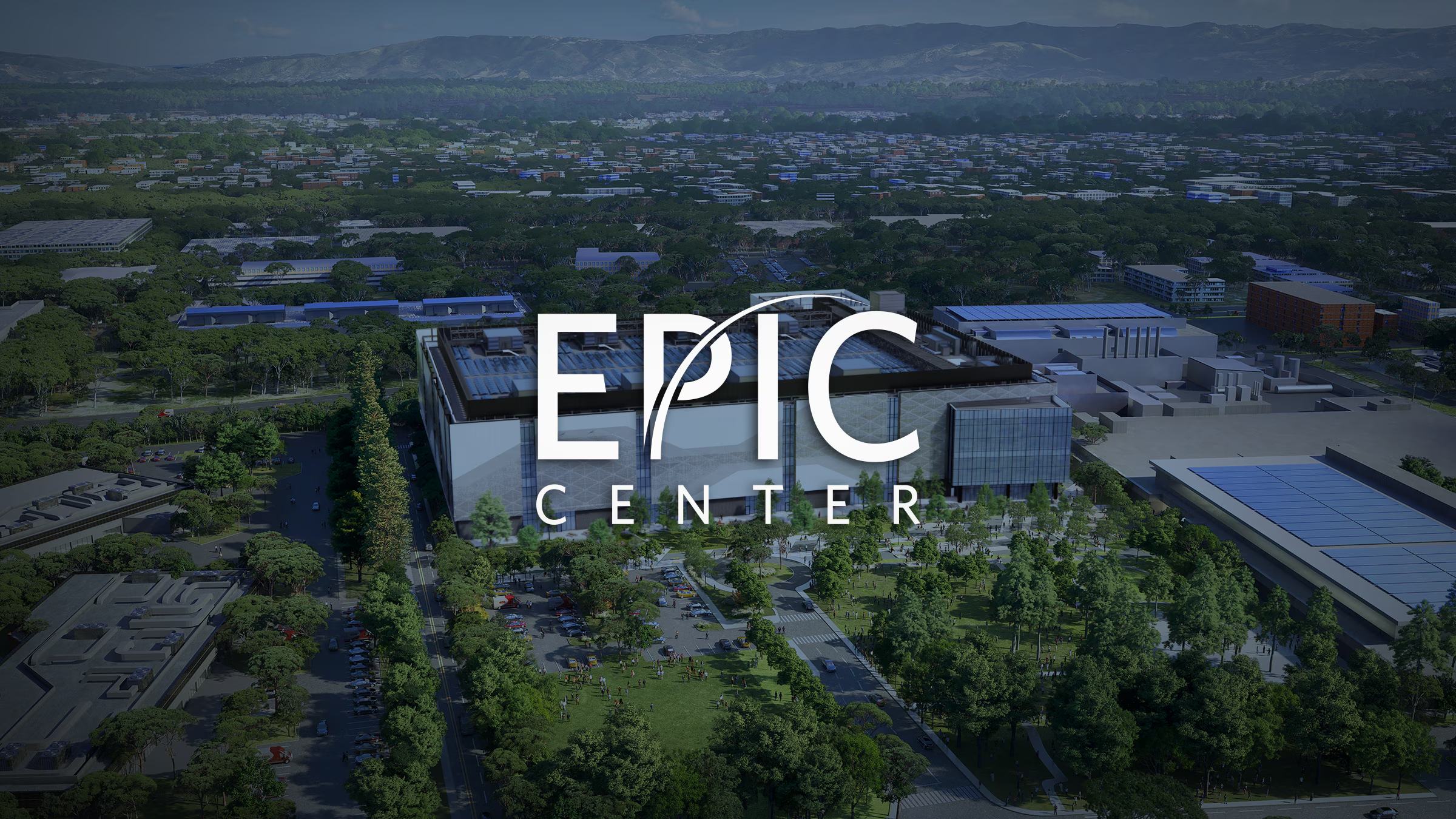
Applied Materials and TSMC have officially announced a new innovation partnership centered on the EPIC Center in Silicon Valley, a major 5 billion$ research and development hub designed to accelerate the semiconductor technologies needed for the next wave of AI chips. The companies say they will work together on materials engineering, equipment innovation, and process integration to speed up the path from early research to high volume manufacturing, with a specific focus on the increasingly difficult scaling challenges now facing advanced logic designs.
This matters because the next phase of AI hardware is no longer just about pushing smaller nodes in a traditional way. Applied Materials and TSMC are explicitly targeting some of the toughest bottlenecks in the roadmap, including the formation of more complex 3D transistor and interconnect structures, as well as the process integration work needed to improve yield, variability control, and long term reliability as chips move toward vertically stacked and highly scaled architectures. In practical terms, this is about solving the manufacturing complexity that comes with trying to keep AI performance and efficiency moving forward at the data center and edge.
Applied Materials says the EPIC Center represents the largest ever United States investment in advanced semiconductor equipment research and development, with capital spending expected to scale over time to around 5 billion$ as customer projects ramp up. The company also says the site will be operationally ready this year and has been built to shorten the time required to move breakthrough technologies from lab stage research into full scale manufacturing. That gives TSMC earlier access to Applied’s research teams, tools, and development pipeline as both companies work on future generation process readiness.

The companies are framing this as an extension of more than 30 years of collaboration, but the tone of the announcement also shows how much the AI era is changing the stakes. Applied Materials CEO Gary Dickerson said the partnership is meant to address the “unprecedented complexity” now driving the chipmaking roadmap, while TSMC Executive Vice President and Co Chief Operating Officer Dr. Y.J. Mii said that the increasing demands on materials engineering and process integration require broader industry collaboration to meet AI scale challenges. That language makes it clear this is not just another routine supplier customer arrangement. It is a deeper co innovation move aimed at the heart of future semiconductor scaling.
Applied also outlined 3 main technical focus areas for the work with TSMC. The first is process technology that can continue improving power, performance, and area at leading edge logic nodes. The second is the development of new materials and new manufacturing equipment for more precise 3D transistor and interconnect formation. The third is more advanced process integration to maintain yield and reliability as device structures become more vertically complex. Those priorities line up directly with the manufacturing problems that matter most for advanced AI accelerators and high performance computing chips.
For the industry, this partnership is a meaningful signal. The AI boom is pushing chipmakers beyond the limits of straightforward scaling, and more of the competitive battle is now shifting into packaging, interconnect design, materials science, and integration discipline. By placing TSMC inside Applied Materials’ EPIC Center model as a founding partner, both sides are effectively trying to reduce the lag between breakthrough process ideas and deployable manufacturing solutions. That could become one of the most important advantages in the race to build more efficient AI silicon over the next several years. This reading is an inference based on the official partnership scope and the specific technology focus areas outlined in the announcement.
The official announcement from Applied Materials is available through the company’s investor relations release.
Do you think partnerships like this will matter more for future AI chip progress than raw node shrinks alone?