
TSMC Longtan Expansion Moves Forward With 1.4 nm and Future Angstrom Class Fabs Planned

TSMC’s long term manufacturing expansion in Taiwan is taking another step forward, with the planned third phase of the Longtan Science Park clearing an important government review. Supply chain information points to the site being reserved for A14 and more advanced Angstrom class manufacturing, potentially giving TSMC additional capacity for technologies beyond its current 1.4 nm roadmap around the end of the decade.
Taiwan’s National Development Council approved the draft expansion plan for the Longtan section of Hsinchu Science Park on September 17. The project covers approximately 104 hectares, with development costs estimated at NT$95.6 billion and around 4,500 jobs expected to be created. However, this is not final approval to immediately begin constructing TSMC fabs. Environmental assessment, land acquisition, development permits, infrastructure work, water, electricity, transport, and local consultation still have to move forward before construction can fully proceed.
Supply chain sources indicate that TSMC could eventually build 3 advanced wafer fabs at the expanded Longtan site, with total investment potentially exceeding NT$1 trillion. The first facility is currently targeted to be completed around 2030 before moving into production preparation. The development is expected to prioritize advanced logic manufacturing rather than the panel level packaging capacity previously associated with the site.
The first stage is reportedly being considered for 1.4 nm class A14 capacity, while later construction could support enhanced A14 derivatives and technologies beyond that generation. This does not mean Longtan will become TSMC’s first A14 production base. The company is already building a much larger A14 complex in Taichung, where construction on the first facility has progressed ahead of schedule. Our previous coverage detailed how TSMC A14 production could potentially begin during 2H 2027 if equipment qualification and the accelerated construction schedule continue as planned.
TSMC’s official roadmap remains more conservative. The company currently schedules A14 risk production for 2027 and volume manufacturing for 2028. According to its official A14 technology roadmap, the process is expected to provide between 10% and 15% higher performance at the same power compared with N2, or between 25% and 30% lower power at the same performance, alongside more than 20% higher logic density.
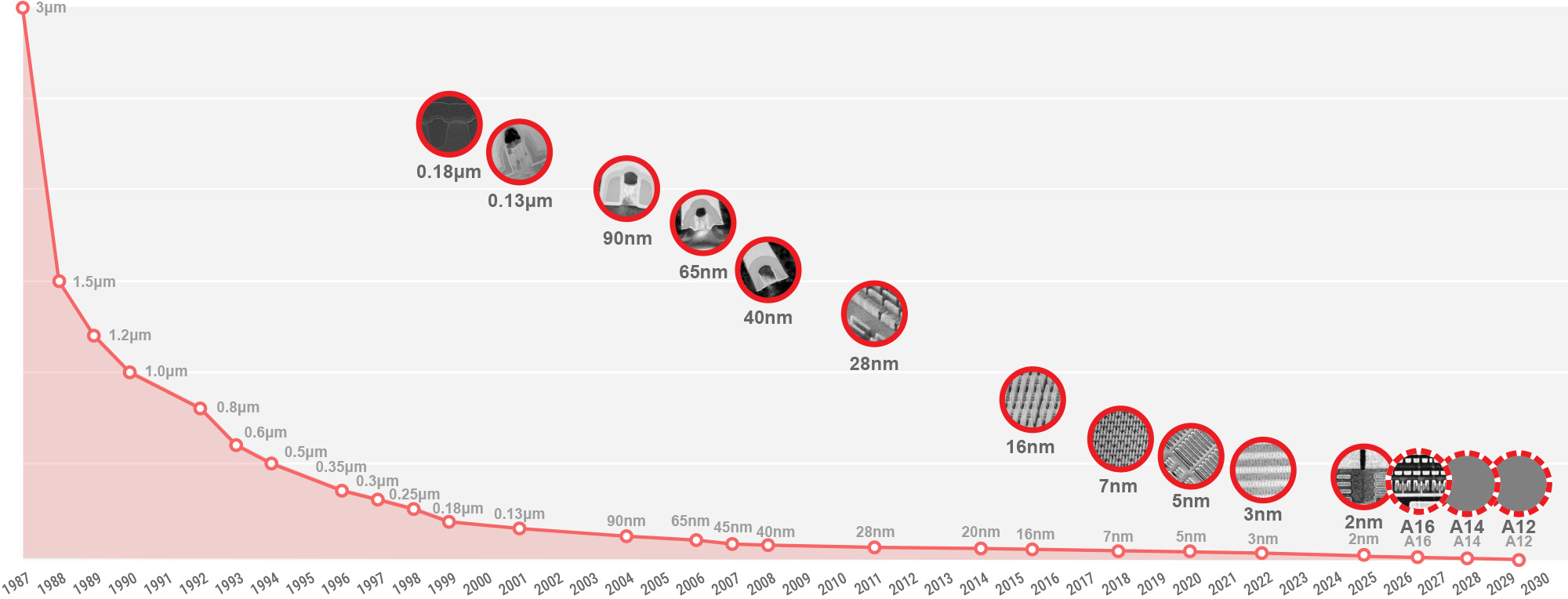
TSMC is already extending that platform further. A13 will use a 97% optical shrink while maintaining design compatibility with A14, while A12 will integrate the company’s Super Power Rail backside power delivery technology. Both are currently scheduled for volume production in 2029. TSMC also lists A12 and technologies beyond it among its future research projects, making the Longtan expansion potentially important well beyond the initial A14 generation.
The expansion comes as competition at the leading edge becomes more intense. Intel is developing its own 14A manufacturing platform for high volume production around 2028. As we previously covered, Intel says 14A defect reduction is progressing faster than any of its process generations since 22 nm, while external companies are beginning to evaluate the platform. Node names cannot be directly compared as physical transistor dimensions, but TSMC A14 and Intel 14A are increasingly shaping up as major competing manufacturing platforms for AI and high performance computing later this decade.
At the same time, TSMC is cautioning against assuming that artificial intelligence can simply accelerate every stage of developing these future nodes. Executive Vice President and Co Chief Operating Officer Y.J. Mii recently explained that AI is already useful for coding, circuit design, and electronic design automation because those tasks generally have more clearly defined inputs and outputs. Advanced process development is different.
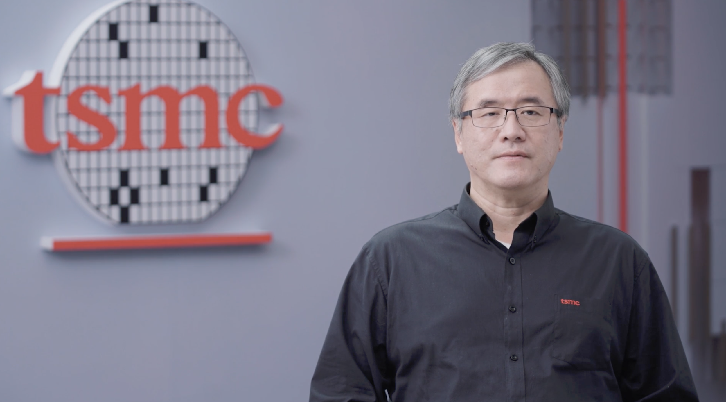
When developing technologies such as A14, engineers are dealing with materials, manufacturing equipment, and physical behavior that may not yet have established solutions or enough historical data for AI models to learn from. Mii explained that AI may suggest possible directions, but it cannot overcome a situation where existing materials or equipment are physically incapable of producing the required result.
"AI can provide a lot of information, suggestions and answers, but the final decision still has to be made by people."
— Quote by: Y.J. Mii.
His comments highlight an important difference between using AI to optimize an existing semiconductor design and using it to invent the manufacturing technology required for a future process. TSMC continues to expand AI use internally, particularly for engineering tasks with clearly defined constraints, but leading edge process research still depends heavily on experimentation, materials science, equipment development, and human engineering judgment.
The Longtan approval is important, but it should not be interpreted as TSMC receiving unconditional permission to immediately construct 3 below 1.4 nm fabs. The project has cleared a major planning stage, while several environmental, land, infrastructure, and utility requirements remain.
What is more interesting is the timeline. Taichung is already becoming TSMC’s first major A14 manufacturing center, while Longtan appears positioned as additional capacity for the later expansion of A14 and whatever follows it. With A12 already scheduled for 2029 and the first Longtan fab potentially preparing for production around 2030, the site could become part of TSMC’s manufacturing foundation for the generation beyond its initial 1.4 nm rollout.
Mii’s comments also provide a useful reality check around AI. Artificial intelligence can accelerate optimization once engineers understand the problem and have usable data, but creating a new transistor, material stack, lithography method, or manufacturing tool still requires solving physical problems that no model can simply calculate away.
Do you think AI will eventually become capable of designing major semiconductor process breakthroughs, or will leading edge manufacturing remain dependent on human led materials and equipment research?
