
TSMC and NYCU Develop 0.42 nm Interface for Future 2D Transistors
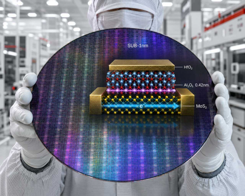
TSMC and researchers from National Yang Ming Chiao Tung University have demonstrated a new transistor interface technique that could help extend semiconductor scaling beyond conventional silicon technologies. The research focuses on monolayer molybdenum disulfide, or MoS₂, a two dimensional semiconductor only atoms thick that is being investigated as a potential channel material for future transistor generations. The work was published in Nature Electronics on July 31, 2026.
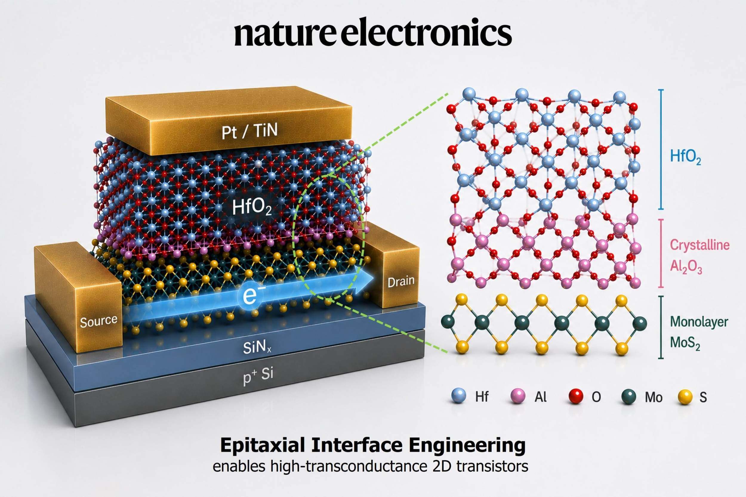
One of the major challenges with two dimensional semiconductors is integrating an extremely thin gate dielectric without damaging carrier mobility. As transistor dimensions continue shrinking, stronger gate control requires a very low equivalent oxide thickness, but conventional dielectric integration can introduce additional scattering at the interface and reduce electron mobility. The TSMC and NYCU research instead concentrates on engineering the boundary between the semiconductor channel and dielectric rather than replacing the entire material system.
Using ultra high vacuum processing, the researchers deposited an extremely thin epitaxial aluminum layer directly onto a monolayer MoS₂ channel. The aluminum was then oxidized into an aluminum oxide layer measuring approximately 0.42 nm thick before a high κ hafnium oxide gate dielectric was deposited above it. This crystalline aluminum oxide interface provides a more controlled foundation for dielectric growth while helping shield the MoS₂ channel from interactions that would otherwise increase carrier scattering.
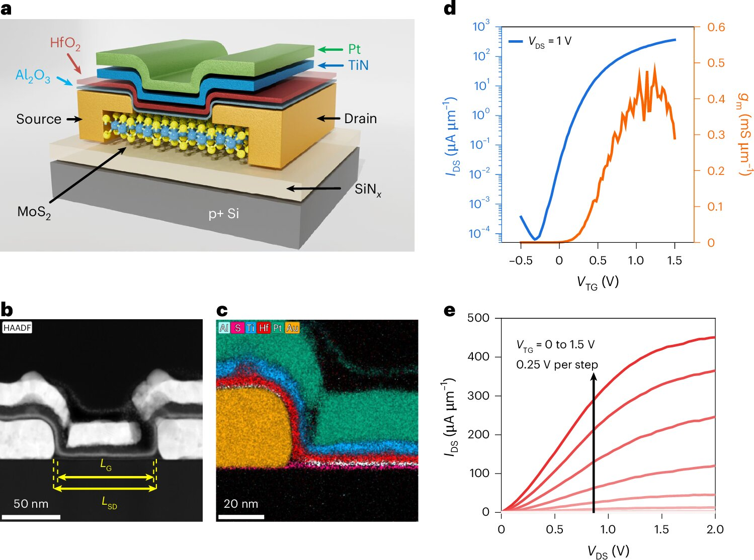
The resulting top gate field effect transistors achieved transconductance of 0.45 mS per μm while maintaining an equivalent oxide thickness of approximately 1 nm. Transconductance is an important transistor performance metric because it represents how effectively the gate voltage controls current through the channel, influencing switching performance, voltage gain, and bandwidth. Achieving high transconductance while simultaneously preserving mobility and aggressively scaling the dielectric has remained one of the major difficulties facing two dimensional transistor development.
"The real competition in future 2D semiconductors is not just materials, but interface engineering."
— Quote by: Professor Wen Hao Chang.
The 0.42 nm measurement requires important context. The researchers have not created a commercial 0.42 nm manufacturing node, nor does the result mean TSMC is preparing 0.42 nm processors. The figure describes the approximate thickness of the aluminum oxide interface used inside the experimental transistor. Modern manufacturing node names also no longer correspond directly to a single physical transistor dimension. The breakthrough instead demonstrates one possible technology that could help transistor scaling continue as conventional silicon channels approach increasingly difficult physical limits.
This research sits considerably beyond TSMC's current production roadmap. The company's N2 technology entered volume production in Q4 2025 using nanosheet transistors, while its A14 process is scheduled to begin production in 2028. A14 is expected to deliver up to 15% higher performance at the same power or up to 30% lower power at the same speed compared with N2, alongside more than 20% higher logic density. Two dimensional materials such as MoS₂ represent a possible technology direction further into the future rather than an immediate replacement for those silicon based platforms.
The development also adds another path to the increasingly competitive race beyond conventional nanosheet scaling. We previously covered TSMC preparing for future 1 nm class manufacturing, while IBM recently demonstrated its own 0.7 nm class NanoStack research technology. These technologies take different approaches, but they highlight how the semiconductor industry is increasingly combining new transistor architectures, materials, interface engineering, and vertical integration rather than relying exclusively on traditional dimensional shrinking.
The most important part of this breakthrough is not the headline grabbing 0.42 nm measurement. It is that TSMC and NYCU have demonstrated a possible way to preserve the electrical advantages of an atomically thin semiconductor while still integrating the extremely aggressive dielectric structures required for future logic.
MoS₂ and other two dimensional materials have looked promising for years, but producing a good semiconductor channel is only part of the challenge. Contacts, dielectrics, interfaces, manufacturing consistency, wafer scale integration, and yield all need to work together before these materials can move from research laboratories into commercially manufactured CPUs, GPUs, and AI accelerators.
TSMC participating directly in this research makes the development particularly interesting because manufacturability will ultimately decide whether two dimensional transistors become part of the post silicon roadmap. This is not a sub 1 nm consumer chip yet, but it addresses one of the engineering barriers that must be solved before those future technologies become practical.
Could two dimensional materials such as MoS₂ eventually replace silicon inside future CPUs and GPUs, or will advanced silicon transistor architectures remain dominant beyond the 1 nm era?
