
IBM Unveils World’s First 0.7 Nanometer Nanostack Chip Technology

IBM has unveiled what it describes as the world’s first sub 1 nanometer semiconductor technology, introducing a 0.7 nm process generation built around a new three dimensional transistor architecture called NanoStack. Also identified as the 7 angstrom node, the research breakthrough is designed to extend logic scaling beyond conventional nanosheet transistors while increasing density, performance, and energy efficiency for future artificial intelligence accelerators, cloud infrastructure, mobile processors, and other advanced computing systems.
According to the official IBM announcement, the new technology could place nearly 100 billion transistors inside an area approximately the size of a fingernail, delivering almost twice the density of the 2 nm research chip IBM revealed in 2021. Published projections indicate up to 50% higher performance at the same power or 70% lower power consumption while maintaining similar performance compared with IBM’s 2 nm reference technology. These figures remain research projections rather than benchmarks from a mass produced consumer or data center processor.
"With our new NanoStack architecture, we are reinventing how chips are built."
— Jay Gambetta
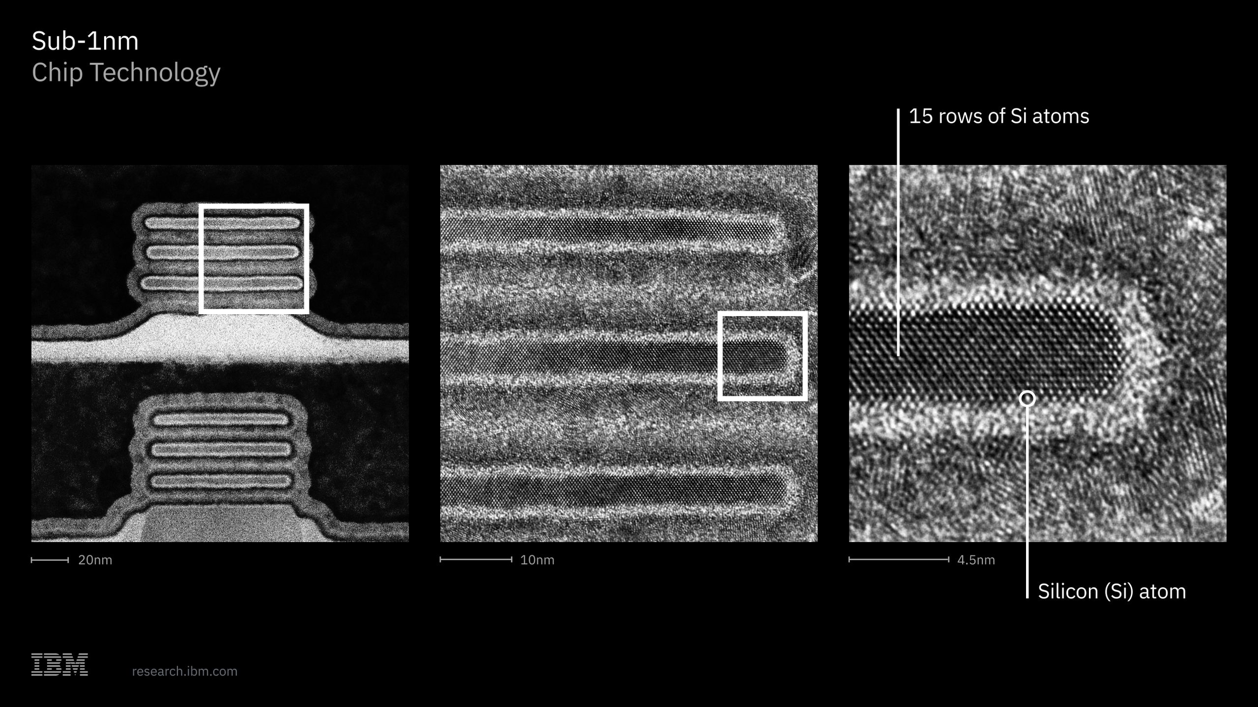
NanoStack moves beyond traditional two dimensional scaling by vertically stacking and staggering nanosheet based transistors. IBM researchers created the structure by bonding 2 wafers through an extremely thin dielectric layer, allowing the upper and lower transistor channels to be positioned with precise alignment. The architecture can also use different channel materials across each layer, giving engineers greater freedom to optimize individual transistors for performance or efficiency. IBM says the design has been experimentally validated through CMOS integration, dual channel engineering, and functional inverter operation.
The underlying NanoStack research paper describes a sequential integration approach in which nanosheet transistors are placed above other nanosheet transistors with extremely small vertical separation. This allows chip designers to increase density by expanding into the vertical axis rather than relying entirely on smaller dimensions across the surface of the silicon. IBM also demonstrated approximately 40% SRAM area scaling, an important improvement because on chip memory occupies a substantial portion of modern processors and has become increasingly critical for artificial intelligence workloads.
IBM estimates that an artificial intelligence accelerator built with the technology could theoretically reach around 9,000 trillion operations per second, compared with approximately 1,500 TOPS for the example accelerators used in its projection. The company also suggests that the additional efficiency and performance could reduce the training time of certain frontier models from approximately 3 months to several weeks. These numbers illustrate the possible benefits of the node and are not measured results from a complete production accelerator.
The 0.7 nm designation also requires context. Modern node names no longer correspond directly to one physical transistor dimension, and IBM itself clarifies that 7 angstrom identifies a generation of manufacturing technology rather than a literal 0.7 nm wire or gate measurement across the complete design. The company currently views NanoStack as a research platform capable of supporting several future generations, with possible commercial adoption beginning within approximately 5 years.

The breakthrough was developed through IBM’s semiconductor research operations in Albany, New York, where the company works with equipment and materials partners including ASML, Lam Research, Tokyo Electron, and SCREEN Semiconductor Solutions. The facility is also preparing for High NA EUV lithography, which is expected to become increasingly important as leading chipmakers move deeper into angstrom class process technologies.
IBM remains primarily a semiconductor research and technology development company rather than a high volume manufacturer competing directly with TSMC, Samsung, or Intel Foundry. Its inventions often influence later commercial processes through research partnerships, licensing agreements, and technology transfers. IBM’s earlier nanosheet research helped establish the architecture now entering production across leading 2 nm and 3 nm platforms.
The NanoStack announcement also intensifies the wider race toward angstrom class manufacturing, TSMC is developing its A14 manufacturing platform for production around 2028, while Intel and Samsung are pursuing their own advanced transistor, backside power, and lithography roadmaps. IBM’s research does not mean the United States has overtaken Taiwan or South Korea in commercial semiconductor manufacturing, but it reinforces the country’s continued strength in foundational chip research and process architecture.
NanoStack is important because it demonstrates that semiconductor scaling may continue after conventional nanosheet designs begin reaching practical limits. By stacking transistors vertically and allowing different channel materials across each layer, IBM is creating additional options for increasing density without depending entirely on smaller horizontal features.
The largest challenge will be transforming a laboratory demonstration into an affordable and reliable manufacturing process. Wafer bonding accuracy, thermal management, material compatibility, defect control, yield, lithography costs, and design software will all determine whether NanoStack can move into high volume production.
IBM has demonstrated a credible direction, but the commercial semiconductor race will ultimately be decided by companies capable of producing millions of advanced chips at competitive yields. The announcement proves that American semiconductor research remains highly influential, while also showing why international manufacturing partnerships will continue to be essential.
Could vertically stacked NanoStack transistors extend semiconductor scaling for another decade, or will manufacturing complexity make the technology too expensive for widespread adoption?