
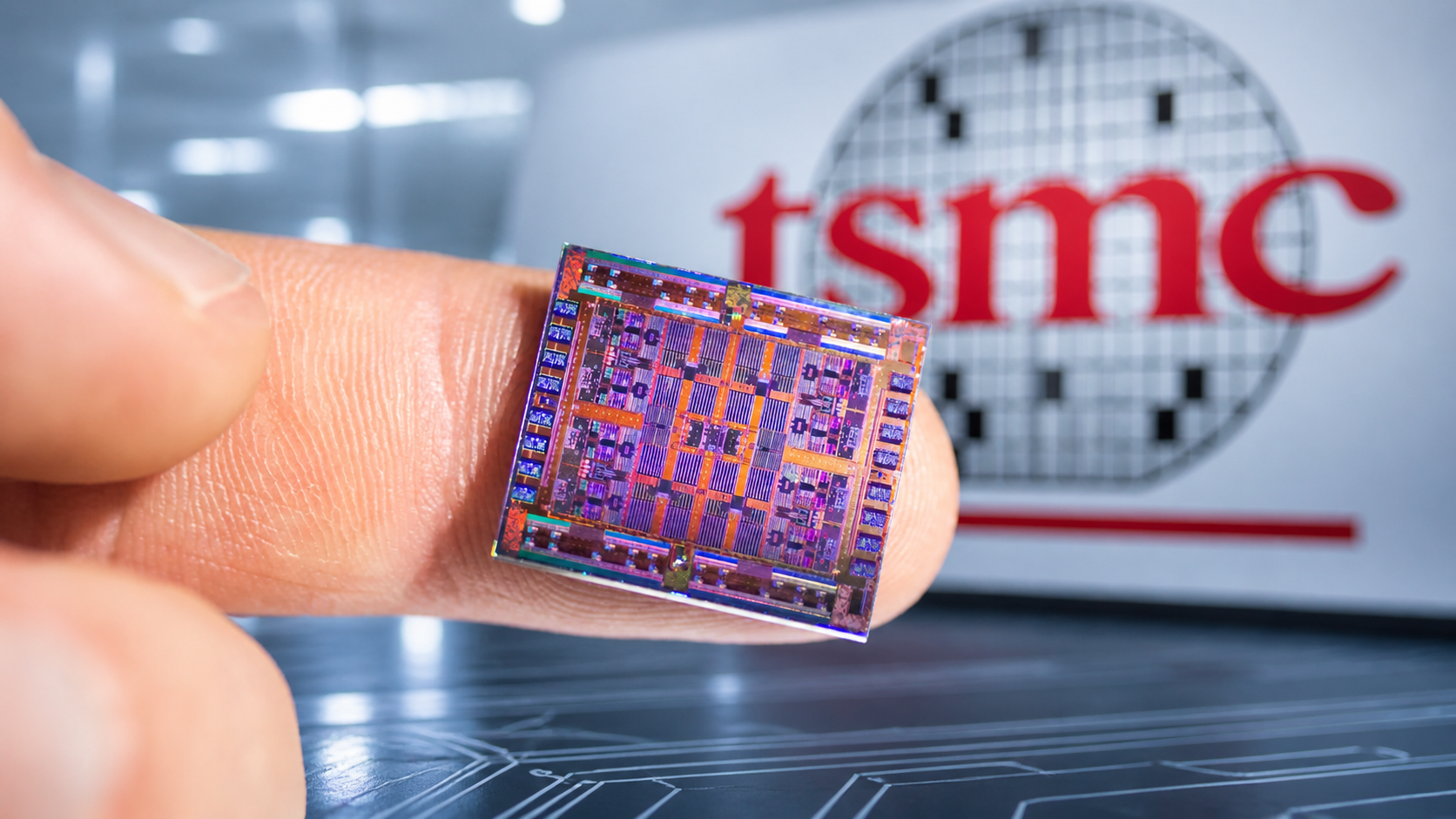
TSMC 2nm Output Reportedly Set To Outpace 3nm By 45% As AI Demand Forces A Faster Ramp
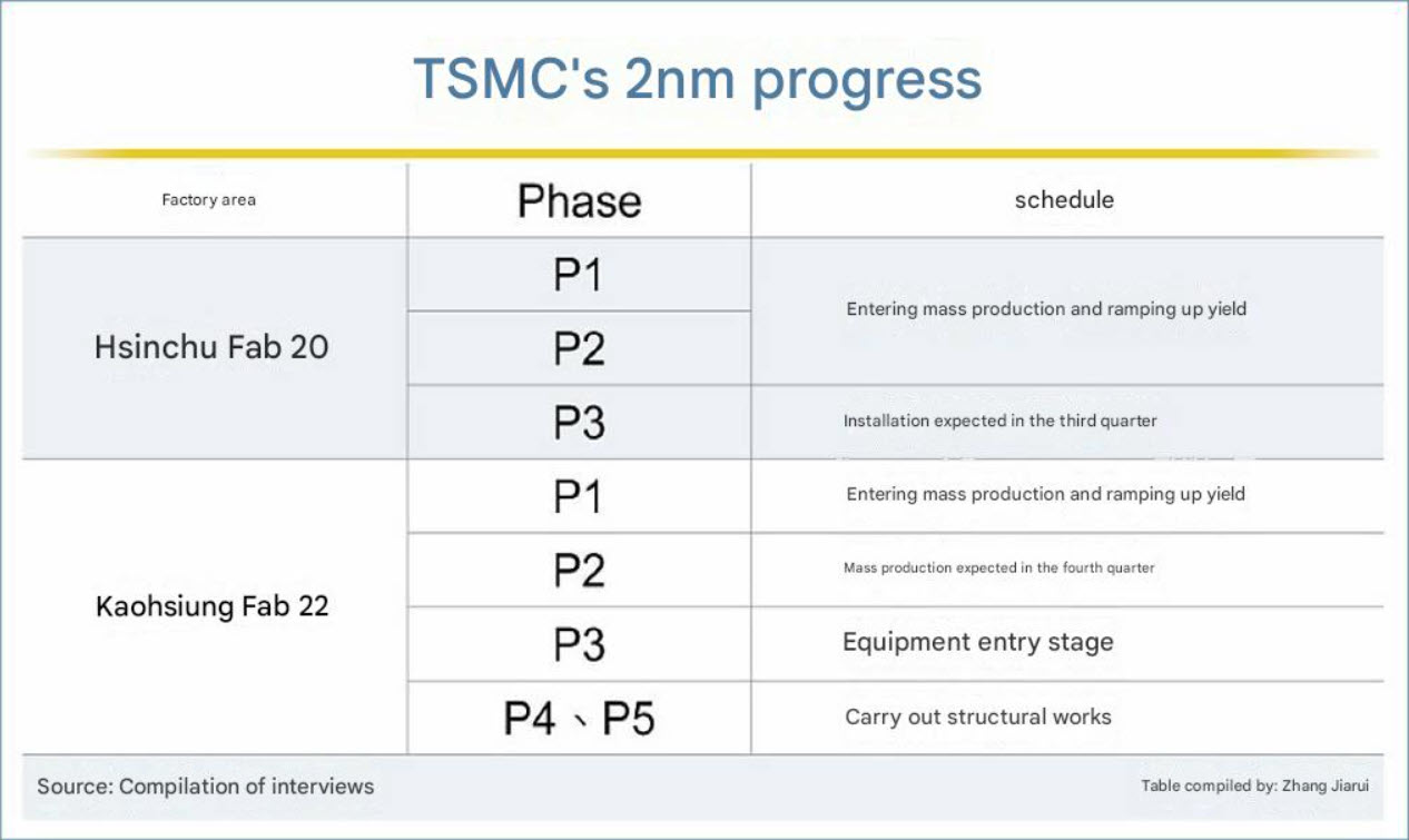
TSMC is reportedly preparing a much more aggressive 2nm ramp than it managed at the same point in the 3nm cycle, underscoring just how intense current demand has become for leading edge process technology as AI and high performance compute customers push for more wafer capacity. According to a report from Commercial Times, TSMC’s 2nm output is expected to be 45% higher than 3nm was at the same stage of production, with 5 fabs tied to the 2nm push entering ramp up this year.
That claim fits the broader direction TSMC has already outlined publicly. On April 17, 2026, TSMC said its N2 technology is scheduled for volume production in the second half of 2026, and described customer interest as “high” across smartphone and HPC applications. TSMC also said it expects the number of new tape outs for 2nm within its first 2 years to exceed both 3nm and 5nm over the same period, which strongly supports the idea that N2 demand is arriving faster and at larger scale than previous major nodes.
The reported 45% figure is especially notable because TSMC is not just scaling the front end. The company has also been investing heavily in advanced packaging and backend capacity to keep pace with AI accelerator demand, an area where larger package sizes and HBM integration are becoming just as important as transistor scaling itself. TSMC has repeatedly highlighted strong demand from HPC and AI customers in its recent investor communications, and those segments now account for a growing share of its revenue mix.
Commercial Times also reportedly says TSMC is building and ramping 5 fabs tied to the 2nm generation while continuing broader global expansion in Arizona, Japan, and Germany. TSMC’s own manufacturing pages and Arizona project materials confirm that international buildout remains active, with the Arizona campus alone planned to produce tens of thousands of wafers per month for customers once fully developed. That does not directly confirm the exact Commercial Times capacity comparison, but it does reinforce that TSMC is scaling globally at the same time it pushes N2 into volume production.
The market logic behind a faster 2nm ramp is straightforward. AI chips are getting larger, package complexity is rising, and more customers want access to the best power efficiency and performance per watt available. If N2 really does come online with meaningfully more capacity than 3nm had at the same stage, that would be a direct reflection of how much more urgently customers now need bleeding edge process access. This is an inference based on TSMC’s public comments about stronger N2 tape out momentum and continued HPC driven demand.
At the same time, it is important to keep the scope of the claim clear. The 45% comparison comes from a media report, not from an official TSMC capacity disclosure. TSMC has publicly confirmed that N2 volume production starts in the second half of 2026 and that customer interest is stronger than in prior node ramps, but it has not publicly published the exact “45% higher than 3nm at the same stage” figure in the sources I could verify.
Even with that caveat, the bigger takeaway remains intact. TSMC is entering its 2nm era with stronger early demand signals than it had for 3nm, and the company is scaling manufacturing and packaging capacity accordingly. If the reported output comparison is even close to accurate, then N2 is shaping up to be one of the fastest and most strategically important process ramps in TSMC’s history.
Do you think TSMC can keep its lead through the 2nm era, or will rising demand finally open the door wider for rivals and alternate foundry partners?