
Tesla Splits AI6 and AI6.5 Across Samsung Texas and TSMC Arizona as Its Next 2nm AI Chips Move Onto US Soil
Tesla’s next generation AI silicon roadmap is taking a more explicit United States manufacturing shape, with Elon Musk indicating that AI6 will be produced on Samsung’s 2nm process in Texas, while AI6.5 will move to TSMC’s 2nm production in Arizona. The update follows Musk’s recent public comments around Tesla’s AI chip pipeline and extends the company’s increasingly visible dual foundry strategy for advanced in house silicon.
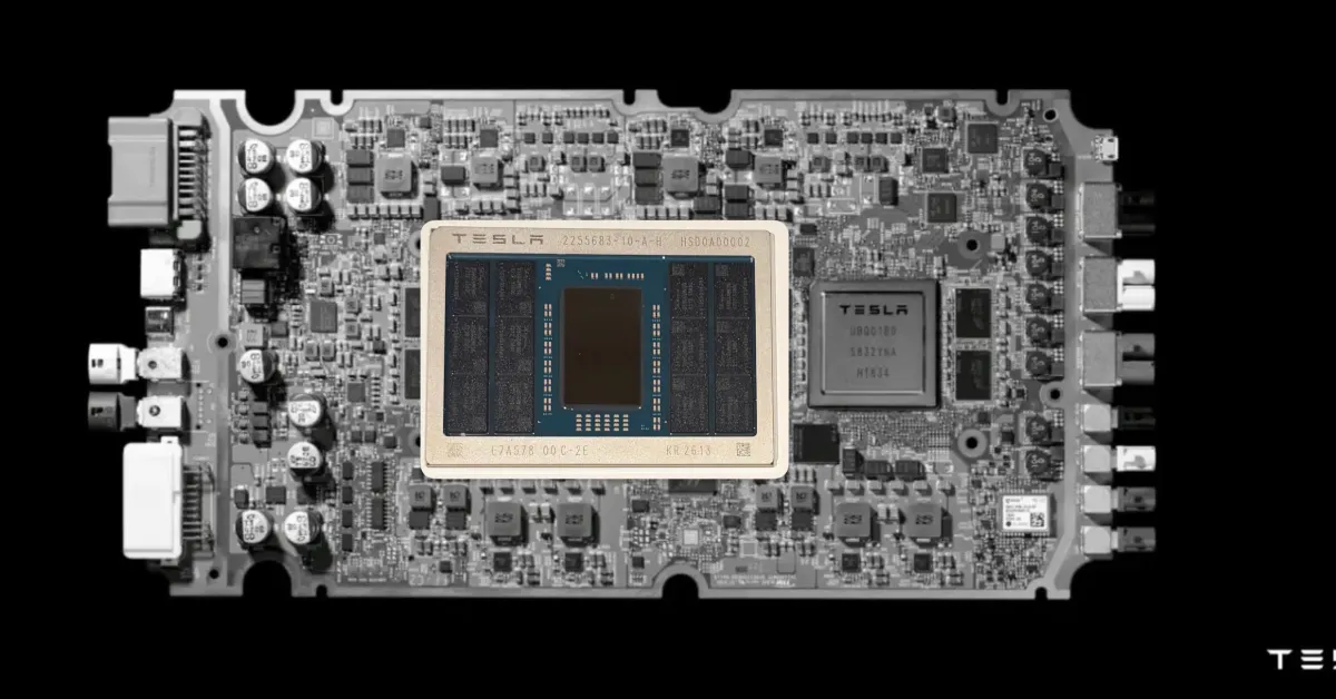
The immediate context is Tesla’s newly completed AI5 tapeout, which Musk described as a meaningful milestone but also one that involved design concessions to accelerate delivery. In his comments, he suggested those compromises were part of why the design reached tapeout ahead of schedule, while also making clear that AI6 is intended to recover some of the architectural goals that AI5 left on the table. Reuters separately reported last month that Musk said Tesla could tape out AI6 by December 2026, with Samsung’s Texas operation expected to handle production for that chip generation.
Best was working with such a great team of AI hardware & software engineers! It was more fun than going to parties on Saturdays by far.
— Elon Musk (@elonmusk) April 15, 2026
Least awesome was that we had to make several design concessions to move fast, but were able to finish tapeout 45 days ahead of schedule.
AI6…
What makes this roadmap especially notable is the structure Tesla appears to be using. Rather than relying on a single foundry partner, the company is spreading its advanced AI chip plans across both Samsung and TSMC, while still keeping production inside the United States. Based on Musk’s latest remarks, AI6 is tied to Samsung Texas, while AI6.5 is positioned as a further optimized follow up built on TSMC Arizona 2nm. That gives Tesla a combination of supply diversification, geographic concentration inside the United States, and access to two of the most important advanced manufacturing ecosystems in the industry.
Musk’s comments also indicate that AI6 is expected to deliver roughly 2 times the performance of AI5, while using LPDDR6 instead of the previous generation memory approach. That memory shift matters because bandwidth and efficiency are becoming central constraints for AI inference and tightly integrated accelerator designs, especially in automotive and robotics workloads where power, thermal limits, and responsiveness all matter.
Another architectural point tied to the new roadmap is Tesla’s emphasis on SRAM centric efficiency. Reporting based on Musk’s posts says AI6 and AI6.5 will reduce the share of TRIP AI computation accelerators dedicated to SRAM, with the intended result being dramatically stronger effective memory bandwidth for workloads that remain within cache. If that design philosophy holds in finished silicon, it would suggest Tesla is trying to sharpen inference efficiency and reduce some of the traditional bottlenecks that come from leaning too heavily on external DRAM bandwidth.
This all fits into a bigger manufacturing picture. Tesla is still pushing toward Terafab as a future in house answer to its growing silicon appetite, but that project remains years away from volume relevance. In the meantime, Musk has already said that his companies will remain important customers of outside foundries because internal demand is simply too large to wait. Splitting AI6 and AI6.5 between Samsung and TSMC while keeping both in US fabs looks like a transitional version of that strategy, one designed to secure capacity now while longer term manufacturing ambitions continue in parallel.
From a strategic point of view, this is one of the more interesting AI hardware moves coming out of Tesla. It is not just about node shrinks or patriotic reshoring messaging. It is about building redundancy, keeping production close to home, and making sure Tesla’s next wave of automotive, robotics, and broader AI compute plans are not trapped behind a single supplier or geography. In a market where advanced capacity is still tight, that kind of split sourcing could become a meaningful competitive advantage.
The larger test, of course, will be execution. Samsung Texas and TSMC Arizona are both central to broader US semiconductor ambitions, but advanced ramp quality, timing, and yields will decide whether Tesla’s roadmap lands cleanly. For now, though, Musk’s message is clear: Tesla’s next major AI chips are being lined up not just on 2nm, but on 2 separate US foundry tracks.
Do you think Tesla’s split between Samsung and TSMC is the smarter long term AI chip strategy, or would a single foundry path be better for execution and consistency?