
Samsung Reaches 900 Layer V-NAND Prototype As 1000 Layer NAND Moves Closer To Reality
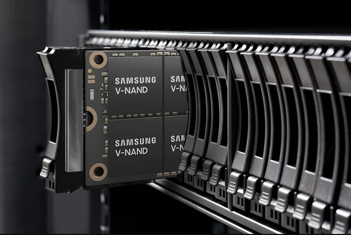
Samsung is moving closer to one of the biggest milestones in storage semiconductor development, with a new report indicating that the company has achieved its first 900 layer V-NAND prototype by combining two 450 layer cell stacks into a single device. According to ETNews, Samsung implemented the new prototype using Cell Multi Bonding, also known as CMB, a technique that bonds two separate 450 layer cell wafers together. This approach allows Samsung to dramatically increase NAND layer count without needing to build the full structure as one single stack from the beginning.
“According to the semiconductor industry on the 25th, Samsung Electronics recently implemented a 900 layer Class V-NAND integrated system utilizing Cell Multi Bonding CMB technology, which bonds two 450 layer cell wafers into one.”
— ETNews
The achievement is still in the prototype stage, but it shows a clear path toward the future of ultra high capacity NAND storage. As SSD demand continues to grow across servers, desktops, laptops, smartphones, gaming systems, and enterprise infrastructure, higher layer counts will become increasingly important for improving capacity, density, and cost efficiency.
Samsung has long been one of the leading companies in V-NAND technology, and the company previously outlined ambitions to reach 1000 layer NAND using new materials and more advanced manufacturing methods. The new 900 layer prototype suggests that Samsung is now much closer to that target, even if commercial deployment is still several years away.
Reaching this level is not simple. As NAND layer counts increase, manufacturing becomes more complex, especially because the wafers can suffer from warping and alignment issues. According to the report, Samsung addressed wafer warping through a new Upper Chuck Design, while misalignment errors were reduced through Overlay Correction technologies.
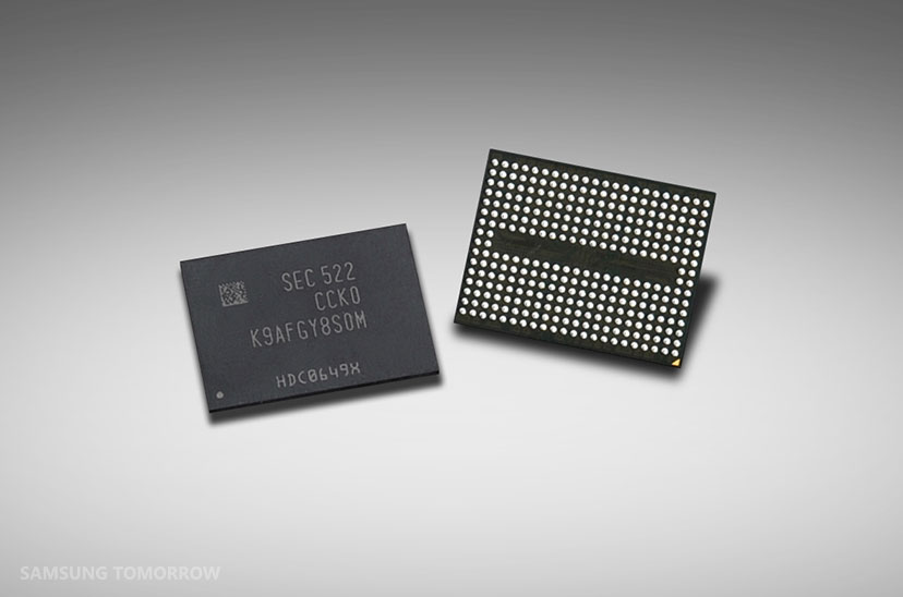
These process improvements are critical because future NAND scaling will depend not only on stacking more layers, but also on maintaining strong yield, precision, and reliability. A small alignment error across hundreds of layers can affect performance, durability, and production efficiency, making bonding and correction technologies essential for next generation NAND development.
The competition is also heating up. SK hynix currently leads in commercial layer count after becoming the first to develop and offer 321 layer NAND. Work is already underway on 400 layer NAND, with Samsung expected to use Vertical Bonding while SK hynix moves forward with Hybrid Bonding.
Chinese NAND manufacturer YMTC is also accelerating its roadmap. The company already offers 294 layer and 232 layer NAND devices and is narrowing the technology gap with Samsung, SK hynix, and Micron. YMTC is also investing heavily in new fabrication capacity, with plans to double wafer output at a time when the global market is under pressure from AI driven demand.
The larger market context is important. AI infrastructure is increasing demand for memory and storage across data centers, cloud platforms, and edge systems. As supply tightens, NAND makers are under pressure to improve density and expand output while keeping costs competitive. Higher layer NAND could help address that challenge by allowing more storage capacity per wafer over time.
Samsung’s 900 layer V-NAND prototype is therefore not just a laboratory achievement. It is part of a broader race to scale storage capacity for the next decade of computing. Enterprise SSDs, AI servers, consumer drives, mobile devices, and gaming platforms could all benefit from higher density NAND once the technology matures.
Commercial 1000 layer V-NAND is currently expected around 2030, while 400 layer plus NAND is expected to roll out in the coming years. If Samsung can successfully move from prototype to production, it could regain stronger momentum in the high density NAND race and reinforce its position as one of the most important storage semiconductor companies in the world.
For now, the key takeaway is clear. Samsung has taken a major step toward 1000 layer NAND, and the future of SSD capacity is moving into a far denser, more complex, and more competitive era.
Do you think 1000 layer NAND will be more important for enterprise AI storage first, or will consumer SSDs benefit from the technology sooner than expected?
