
Intel Foundry’s Rio Rancho Facility Could Become The Global Launchpad For Mass Produced Glass Substrates
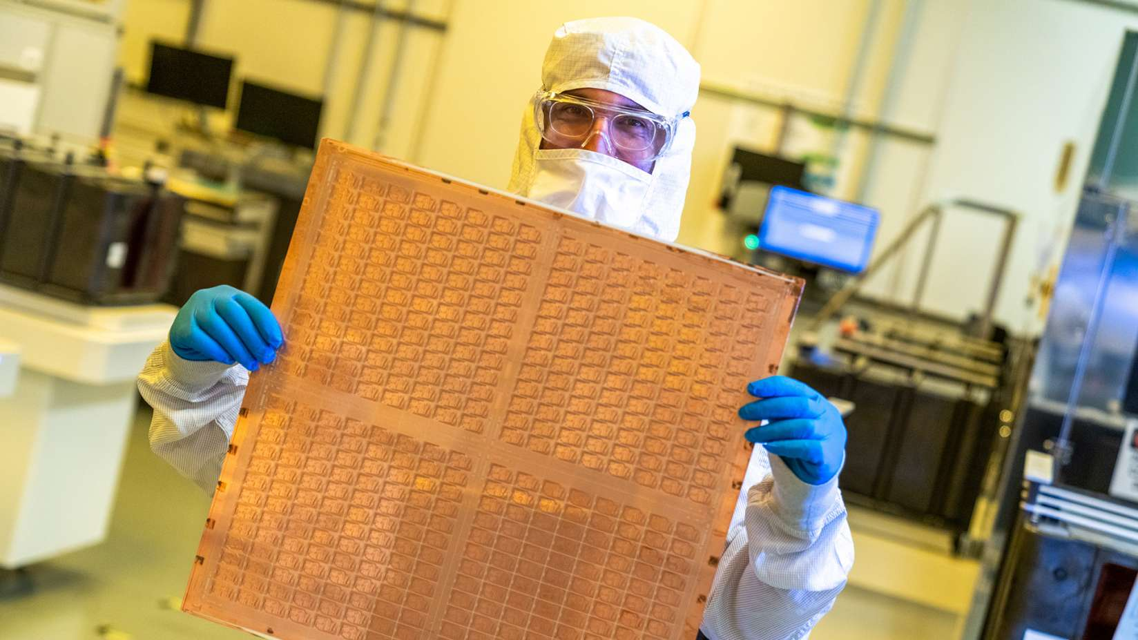
Intel Foundry is positioning its Rio Rancho facility in New Mexico as one of the most important sites in the next phase of semiconductor manufacturing, with new reporting suggesting the plant could become the world’s first location for volume production of advanced glass substrates. Glass core substrates have become a major focus across the semiconductor industry as chipmakers look for alternatives to traditional organic substrates. The pressure is increasing because AI infrastructure demand has tightened supply across advanced packaging materials, while major suppliers such as Ajinomoto have reportedly raised prices as demand grows. This has pushed the industry to search for new packaging technologies that can improve density, reduce limitations, and support more complex chip designs.
Intel first announced its glass substrate roadmap in 2023, positioning the technology as a long term solution for advanced packaging. Compared with traditional organic substrates, glass substrates can help reduce warpage, improve dimensional stability, increase interconnect density, and support more advanced chiplet based designs. These advantages matter more as AI accelerators, data center CPUs, networking chips, and high performance computing processors become larger, denser, and more power hungry.
Earlier this year, Intel showcased its first Glass Core substrate using EMIB Advanced packaging, strengthening its claim that glass could become a major foundation for future heterogeneous chip designs. Since then, the technology has reportedly drawn interest from major companies including Apple and Tesla, both of which have also been connected to Intel Foundry’s advanced process technologies such as 18A P and 14A.
According to Forbes, Intel’s Rio Rancho facility is already manufacturing silicon photonics for external customers. That is strategically important because silicon photonics and Co Packaged Optics are expected to reshape data center infrastructure by replacing parts of traditional copper based interconnect systems with faster and more power efficient optical links.
The combination of glass substrates, silicon photonics, and Co Packaged Optics could become one of Intel Foundry’s strongest differentiators. As AI clusters scale, data movement is becoming one of the biggest performance and power challenges. Faster interconnects, better packaging, and tighter integration between compute and optical communication could help reduce latency, lower power consumption, and improve system level efficiency.
Forbes reports that Intel’s Rio Rancho facility is likely to become not only Intel’s first volume manufacturing site for glass substrates, but potentially the first such site in the world. Intel currently has glass substrate technology available on a pilot line in Chandler, but Rio Rancho is reportedly being prepared for full volume production.
“Most recently, Intel began offering silicon photonics manufacturing at Rio Rancho to its external foundry customers. Rio Rancho is also likely to be not just the first Intel site, but the first site in the world for volume manufacturing of glass substrates, which is currently available only on a pilot line in Chandler.”
— Forbes
The historical significance of Rio Rancho also adds weight to the report. The New Mexico facility opened for manufacturing in the 1980s and became one of Intel’s leading global manufacturing sites during the 1990s and 2000s. Now, the facility may be entering a new era as a core hub for glass substrates, silicon photonics, and advanced packaging.
Intel’s advanced packaging push also comes as the company works to strengthen its Foundry business. While there were previous reports suggesting Intel could consider spinning off its foundry operations, the current direction appears much more ambitious. If Intel can commercialize glass substrates ahead of competitors, it could give the company a valuable advantage in packaging technology even as process node competition remains intense.
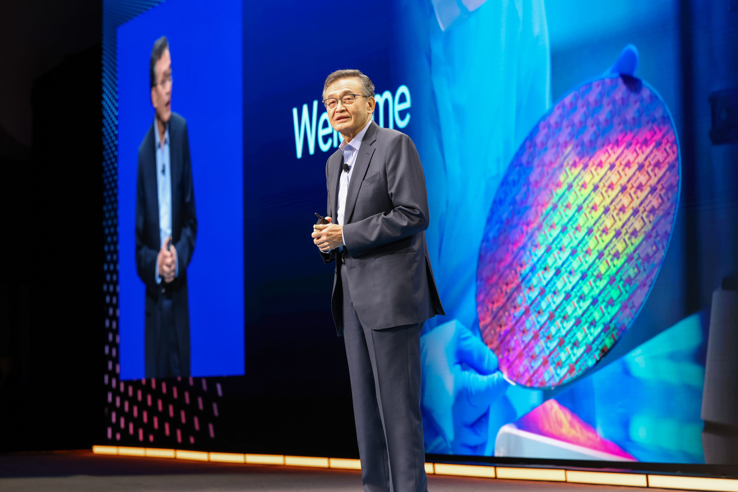
Forbes also reports, citing channel sources, that AWS and Cisco are current customers of Intel Foundry’s advanced packaging services, while Apple, Google, Microsoft, NVIDIA, and Tesla are reportedly engaged in discussions around potential collaborations.
“According to reports from channel sources, AWS and Cisco are current customers of Intel Foundry’s advanced packaging services, while Apple, Google, Microsoft, Nvidia, and Tesla are reportedly engaged in discussions regarding potential collaborations.”
— Forbes
This customer interest matters because advanced packaging is becoming just as strategic as wafer manufacturing. Modern chips are no longer defined only by transistor density. They are increasingly defined by how multiple chiplets, memory, interconnects, optical links, and power delivery technologies are integrated into a single package or system level architecture.
Glass substrates could become especially important for large AI accelerators and data center platforms. As chip packages become larger, traditional organic substrates face more challenges around warpage, signal integrity, power delivery, and routing density. Glass offers a potential path to higher precision and more scalable packaging, which could support future generations of AI and high performance computing hardware.
Intel is not alone in pursuing the technology. Industry partners and packaging leaders are also investing in glass substrate development, and Amkor has indicated that commercialization could arrive within roughly 3 years. That timeline aligns with broader industry expectations that advanced packaging will become a key battleground before the end of the decade.
The first prototypes combining glass substrates with Co Packaged Optics have already been shown, with broader rollout targets around 2030. If Intel can move Rio Rancho from preparation to volume production ahead of competitors, it may give the company an early leadership position in a packaging category that could become essential for future AI data centers.
For Intel Foundry, this is a critical opportunity. The company is trying to prove that it can compete not only through advanced process technologies, but also through packaging, photonics, and systems integration. Glass substrates could become one of the technologies that helps Intel build a more differentiated foundry business, especially for customers designing complex AI, networking, automotive, and high performance computing products.
The future of semiconductors is increasingly being shaped by packaging innovation. Smaller process nodes still matter, but data movement, memory bandwidth, interconnect density, thermal behavior, and package level integration are now equally important. Intel’s Rio Rancho facility could become a central piece of that future if it successfully becomes the first site to mass produce glass substrates.
Do you think glass substrates will become Intel Foundry’s biggest advantage in advanced packaging, or will competitors catch up before the technology reaches mass adoption?
