
Google Reportedly Eyes a Two Chip TPU Inference Strategy With Marvell to Push Memory Efficiency and Next Generation ASIC Performance
Google may be preparing a notable expansion of its custom AI silicon strategy, with a new report claiming the company is in talks with Marvell to develop 2 separate chips focused on inference. According to The Information, one of the proposed chips is a memory processing unit designed to work alongside Google’s existing TPU infrastructure, while the other is described as a new TPU built specifically for running AI models. That pairing suggests Google is not just looking at more raw accelerator performance, but at a broader redesign of how memory and inference workloads are handled across its ASIC stack.
If that report proves accurate, the most important element may actually be the memory side rather than the TPU itself. A dedicated memory processing unit would imply that Google is looking for ways to reduce bottlenecks around bandwidth, data movement, and inference efficiency without relying only on larger or more expensive monolithic accelerators. Inference increasingly depends on memory behavior as much as compute throughput, especially when models become larger, context windows grow, and agent style systems need to keep latency under tighter control. The reported MPU approach looks like an attempt to move some of that burden into a more specialized component.
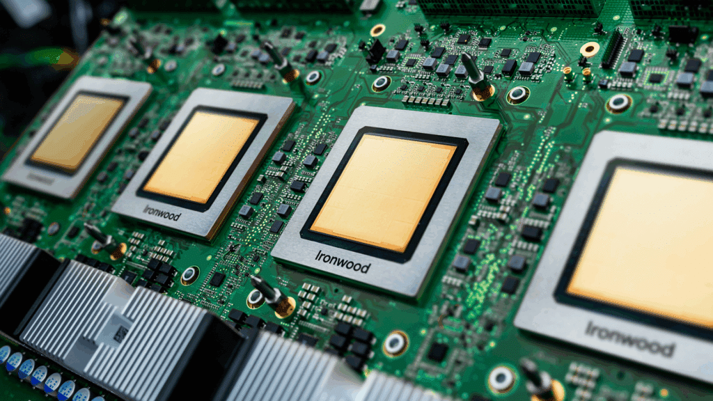
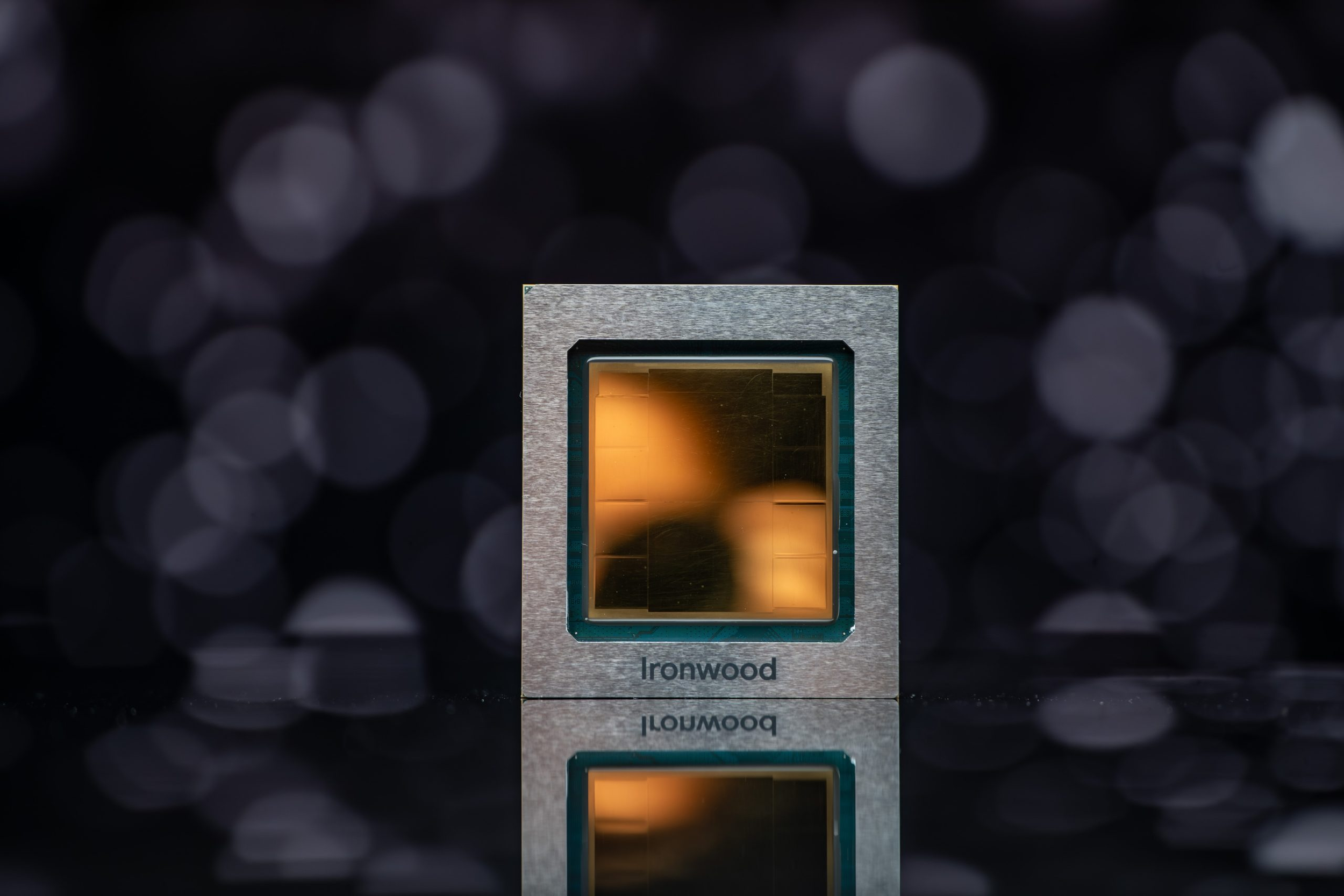
The second chip in the report, a new inference focused TPU, would fit neatly into Google’s current AI infrastructure trajectory. Google has already positioned its latest Ironwood TPU, sometimes referred to as TPU v7, as a major step forward for large scale AI workloads. Google says Ironwood delivers 192 GB of HBM per chip, 4,614 TFLOPS of peak compute, and scales into a 9,216 chip pod configuration. Those figures underline just how serious Google already is about custom silicon at hyperscale, but they also show why the company might now be looking for more specialized inference designs rather than relying on a single do everything accelerator approach.
That is also why this rumored Marvell partnership matters beyond one product cycle. A memory centric companion chip plus a more targeted inference TPU would signal a move toward a more disaggregated ASIC architecture, where different pieces of the inference pipeline are assigned to more purpose built silicon. That is broadly in line with where the market is heading. The biggest AI infrastructure players are no longer just competing on bigger chips. They are competing on how efficiently they can break down the workload across compute, memory, interconnect, and serving layers. This is where a company like Marvell becomes strategically relevant, because it already has deep experience in custom silicon and data infrastructure partnerships.
The memory optimization angle also has echoes elsewhere in the industry. As a reference point for this broader trend, NVIDIA’s Groq 3 LPU work around low latency inference emphasizes exactly how central on chip memory and SRAM bandwidth have become. NVIDIA says each Groq 3 LPU accelerator delivers 500 MB of SRAM and 150 TB per second of SRAM bandwidth, while the rack scale LPX system reaches 40 PB per second of total SRAM bandwidth. That does not mean Google is copying the same design philosophy, but it does reinforce the core market direction: inference is increasingly about getting data to the right place at the right time, not just about maximizing headline FLOPS.
There is also a wider supplier story in the background. Google has long worked with Broadcom around TPU related infrastructure, and earlier reporting from The Information showed that Google had at least explored reducing reliance on Broadcom in parts of its TPU server chip ecosystem. If Marvell is now being drawn into a 2 chip inference effort, it could indicate that Google wants a broader supplier mix as its AI silicon roadmap becomes more segmented and more specialized. That does not necessarily mean a supplier replacement is imminent, but it does suggest Google is keeping its options open as TPU demand continues to rise.
From a competitive standpoint, this could become one of the more important ASIC developments to watch. Hyperscalers are under pressure to lower inference cost, improve token responsiveness, and keep more of the value chain in house. If Google can pair its TPU platform with a memory oriented companion design that meaningfully improves efficiency, it could strengthen its position not only against GPU heavy competitors, but also against other hyperscaler ASIC programs that are trying to carve out their own inference advantages.
For now, it is still a reported discussion, not a formal product launch. The Information says talks are underway, but there is no public confirmation yet from Google or Marvell on final chip definitions, timelines, or production plans. Even so, the reported structure is revealing. Google appears to be thinking beyond a single next TPU and toward a more layered inference architecture, one where memory handling becomes a dedicated silicon priority rather than a secondary design constraint. If that is where this goes, the TPU ecosystem could end up looking much more modular and much more specialized in the next phase of AI infrastructure.
Do you think a memory processing companion chip is the smarter next step for AI inference, or will raw accelerator scale still matter more than specialized memory optimization?