
NVIDIA Feynman Rumors Point to a GTC 2026 Debut and a Potential First Step Toward Groq LPU Adoption
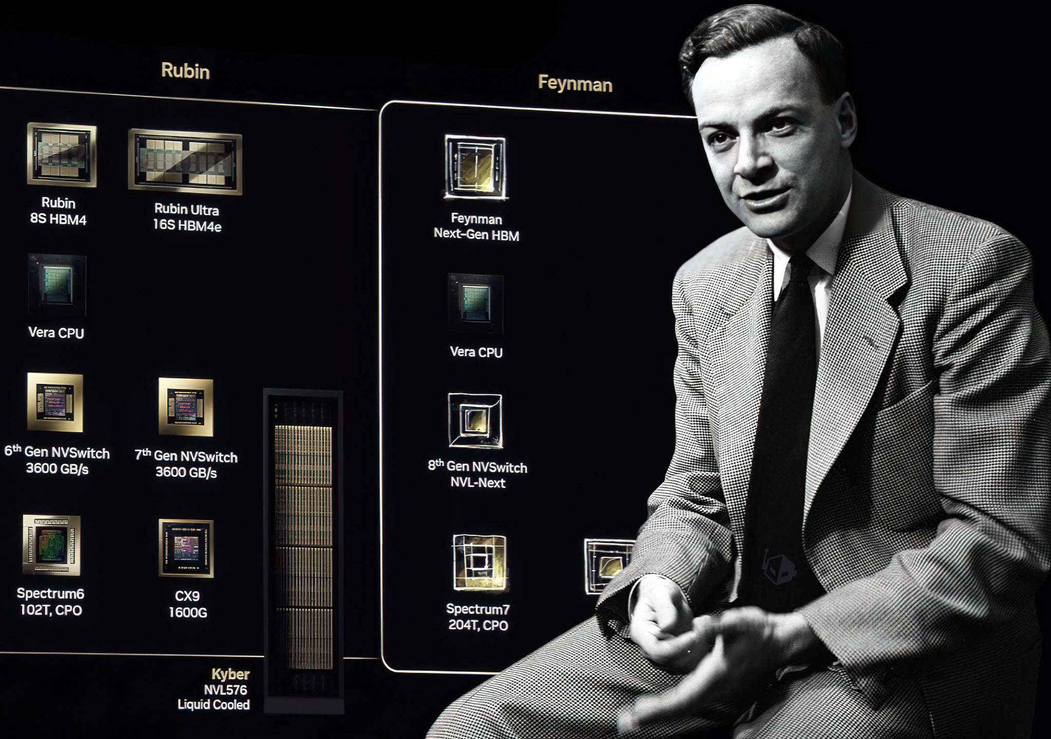
NVIDIA is setting expectations sky high ahead of this year’s GTC, with Jensen Huang teasing that the keynote will feature technology never unveiled before. Now a new report from Chosun Biz is adding fuel to the speculation cycle, claiming that GTC 2026 will mark the first public debut of NVIDIA’s next major chip platform, Feynman. If accurate, this positions GTC as more than a roadmap refresh and more like a strategic tone setter for the next decade of AI compute, especially as hyperscalers and enterprise buyers push harder for better efficiency, lower latency, and more predictable total cost of ownership.
According to the reporting, details on Feynman remain limited, but the headline implication is significant: Feynman could be the first NVIDIA platform tied to TSMC’s A16 process, described as a 1.6nm class node that introduces Super Power Rail and a major step forward in semiconductor scaling. The same report suggests NVIDIA could be TSMC’s first customer for A16 during the early high volume manufacturing phase, with other segments, including mobile, potentially adopting later due to the architectural revamps such a transition may require. In practical terms, the subtext is that NVIDIA may be positioning itself to secure process leadership as a competitive moat, even as the broader industry faces longer lead times and more complex co design between silicon, packaging, and software.
Where this rumor gets especially spicy for AI inference is the secondary angle: the possibility that Feynman might be NVIDIA’s first platform to integrate Groq style LPU units as part of a broader hybrid compute strategy focused on latency. As agentic workloads and real time inference become board level priorities, the bottleneck is increasingly shifting from raw throughput into response time consistency, especially at scale. The theory here is that NVIDIA could explore an advanced packaging approach where LPU blocks complement GPU compute, potentially using bonding and stacking strategies similar in spirit to what the industry has seen in other performance focused designs. The upside is clear: tighter control of inference latency characteristics. The tradeoff is equally clear: dramatically higher complexity in design validation, packaging yields, thermal constraints, and platform software integration.
If NVIDIA does show Feynman at GTC 2026, the shape of the presentation may follow a familiar playbook: a capability rundown, a high level architecture overview, and an early framing of manufacturing timelines rather than a full product launch. Based on the expectations laid out in the report and the broader cadence NVIDIA has used for major transitions, production is being anticipated around 2028, with customer shipments potentially landing across 2029 to 2030 depending on strategy, capacity, and platform readiness. That timeline matters because it suggests Feynman is not just another iteration, it is a longer horizon bet on process leadership and potentially new compute composition.
GTC 2026 begins on March 15, 2026, returning to San Jose, California, and if the Feynman rumor is accurate, this could be the first real signal of how NVIDIA plans to evolve beyond classic GPU centric scaling into a more heterogeneous on package future where latency is treated as a first class product metric rather than an afterthought.
If NVIDIA does reveal Feynman at GTC 2026, would you rather see a pure next gen GPU platform first, or a heterogeneous design that mixes GPU compute with LPU style blocks to chase ultra low latency inference?