
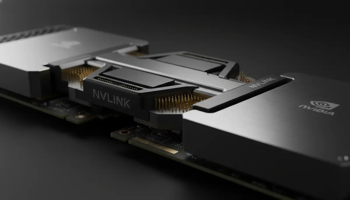
NVIDIA is exploring the use of polytetrafluoroethylene (PTFE), commonly associated with the Teflon coating used in nonstick cookware, to improve signal transmission in its next generation AI server infrastructure. According to a report from Taiwan's Business Today, the company is evaluating PTFE as a potential replacement for conventional insulating resins in high speed NVLink switch boards, where increasing data transfer requirements are creating significant challenges for electrical signal integrity.
The development follows NVIDIA's demonstration of an NVLink PTFE switch board prototype at the October 2026 Open Compute Project Global Summit. The company showcased the technology alongside 7 potential supply chain partners, including Taiwan's Flexium and Taiflex, China's Kinwong, SCC, SYTECH, and VGT, and US manufacturer TTM Technologies. According to DIGITIMES, the demonstration highlights growing interest in alternative printed circuit board (PCB) materials as AI infrastructure moves toward increasingly complex computing systems.
The primary advantage of PTFE comes from its extremely low dielectric loss, allowing high frequency electrical signals to travel through circuit boards with less attenuation than many conventional resin materials. As AI interconnects approach transmission speeds of 200 Gbps per lane, maintaining signal quality becomes increasingly difficult, particularly across long copper traces and complex multilayer boards. Industry sources suggest NVIDIA could eventually integrate PTFE into Rubin Ultra NVLink switch boards or next generation orthogonal midplane designs, potentially reducing reliance on extensive copper cabling.
The technology could complement NVIDIA's existing NVLink 6 architecture, which delivers up to 3.6 TB/s of bidirectional bandwidth per GPU and 260 TB/s across a 72 GPU Vera Rubin NVL72 rack. However, those figures represent the published NVLink 6 capabilities and are not performance improvements attributed to PTFE.
PTFE vs Conventional PCB Materials
| Specification | Conventional High End PCB | PTFE Based PCB |
|---|---|---|
| Dielectric Loss | Higher, material dependent | Very low |
| Signal Integrity | Increasing challenges at high frequencies | Potentially lower attenuation |
| Layer Bonding | Established manufacturing processes | More difficult adhesion |
| Drilling and Plating | Mature production methods | Requires specialized processing |
| Manufacturing Maturity | Established mass production | Advanced AI board designs under evaluation |
| Production Cost | More predictable | Potentially higher |
Despite its electrical advantages, PTFE presents considerable manufacturing challenges. Its low surface energy makes bonding multiple layers difficult, while its relatively soft structure complicates drilling, copper plating, and mechanical processing. Industry estimates cited by Business Today suggest that yields for emerging PTFE AI board manufacturing processes can fall below 5%, although these figures have not been independently validated and do not represent all existing PTFE circuit board technologies. Manufacturers are therefore experimenting with hybrid designs that combine PTFE signal layers with more conventional materials to improve production reliability.
The manufacturing challenges have also created disagreement among PCB suppliers. Some industry executives question whether PTFE can become commercially viable for extremely complex server boards, while others argue that increasingly demanding signal requirements make its adoption necessary. Analysts believe processing limitations could improve over the next 2 years, although the broader commercial outlook may not become clear until 2028 to 2030. NVIDIA has not confirmed a production schedule or final PTFE implementation for Rubin Ultra.
NVIDIA's interest in PTFE highlights an important shift in AI hardware development, where improving GPU performance is no longer sufficient without equally advanced interconnect technology. As data centers expand into increasingly dense computing systems, PCB materials, signal integrity, and manufacturing precision are becoming critical factors in overall infrastructure efficiency. PTFE could provide a meaningful electrical advantage, but extremely low manufacturing yields would make widespread adoption economically difficult. Hybrid PCB designs may offer a more practical transition while manufacturers improve production processes. Ultimately, the next major AI hardware breakthrough may depend as much on materials engineering as on semiconductor architecture.
Could PTFE become the next major breakthrough in AI server connectivity, or will its manufacturing complexity prevent it from replacing conventional PCB materials?
