
NVIDIA Develops Next Generation Optical Interposer Technology With 256 Gb/s Fiber Links
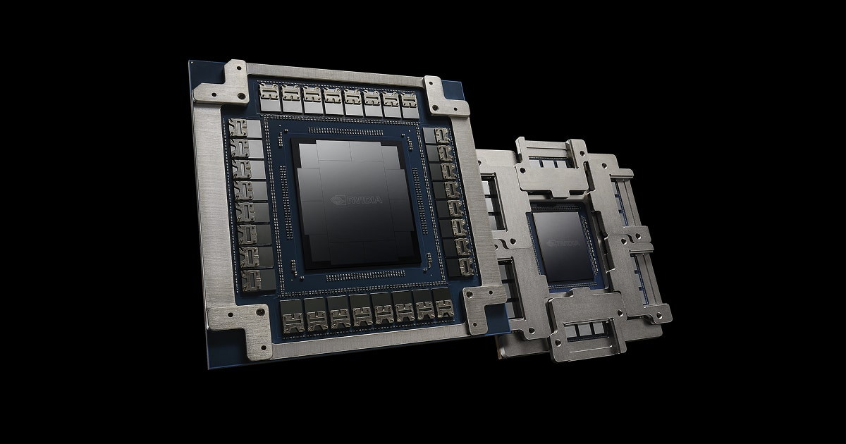
NVIDIA has demonstrated a new approach to co packaged optics (CPO) that brings optical engines directly onto a silicon interposer, potentially increasing communication bandwidth while reducing power consumption in future AI accelerators. The company has also revealed experimental Dense Wavelength Division Multiplexing (DWDM) technology capable of transmitting 256 Gb/s through a single optical fiber, marking another step toward improving connectivity in increasingly demanding AI data centers.
The developments were presented by NVIDIA researcher Nikola Nedovic during SEMICON West 2026 on October 13, in a presentation titled Optical Integration for the Next Generation of AI. According to The Elec, NVIDIA has already developed a prototype of its new Optics on Interposer (OOI) architecture, which moves optical engines from the conventional package substrate onto the silicon interposer that carries the computing chips.
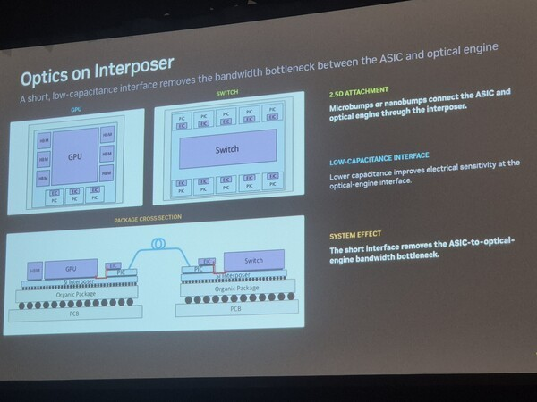
Traditional CPO designs already reduce the distance electrical signals must travel by placing optical engines close to processors or networking ASICs. NVIDIA's proposed architecture goes further by using the interposer's dense, fine pitch electrical connections to communicate directly with those optical engines. This avoids routing the signals through the organic substrate, potentially reducing electrical losses, improving bandwidth density, and lowering power requirements.
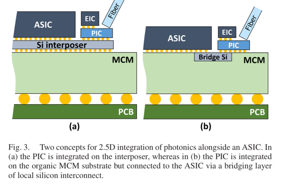
The concept builds on NVIDIA's earlier research into optical integration on silicon interposers, published in 2023. That work examined how shorter electrical connections and wider interfaces could overcome limitations in conventional optical packaging while addressing thermal management challenges.
NVIDIA Optical Interconnect Technology Comparison
| Feature | Current NVIDIA CPO | Next Generation OOI |
|---|---|---|
| Optical Engine Location | Package substrate or optical subassembly | Directly on silicon interposer |
| Electrical Signal Path | Through conventional package interconnections | Shorter interposer connections |
| Bandwidth Density | High | Potentially higher |
| Power Efficiency | Improved over pluggable optics | Further improvements targeted |
| Manufacturing Status | Commercial CPO platforms | Research prototype |
| Main Application | AI networking switches | Future computing and networking packages |
OOI efficiency and bandwidth advantages are research objectives, not verified commercial performance improvements.
Alongside OOI, NVIDIA demonstrated a new DWDM implementation that uses 8 optical wavelengths operating at 32 Gb/s each, delivering an aggregate transmission rate of 256 Gb/s through a single fiber. Rather than increasing the speed of an individual electrical connection, DWDM transmits multiple independent data streams simultaneously using different wavelengths of light. This approach can increase fiber bandwidth while limiting the complexity and power consumption associated with extremely high speed electrical interfaces.
Both technologies remain in development, with NVIDIA identifying thermal stability, packaging complexity, fiber alignment, testing, and manufacturing scalability as obstacles to commercialization. The company has not announced a production schedule or confirmed which future GPU architecture will incorporate OOI or the demonstrated DWDM implementation.
NVIDIA is already introducing conventional co packaged optics through its Quantum X and Spectrum X Photonics platforms. These systems integrate optical engines close to networking processors to reduce reliance on traditional pluggable transceivers, with manufacturing support from partners including TSMC, Coherent, Lumentum, and Corning.
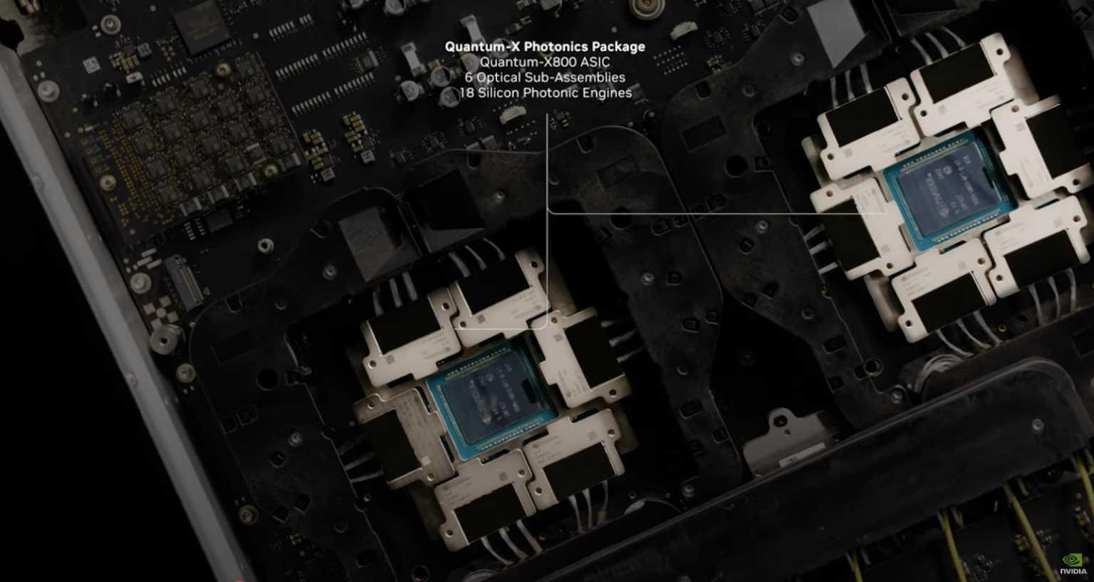
The technology has already demonstrated practical advantages in AI networking. An early Quantum X Photonics switch evaluated by Lambda showed approximately 3.05 kW lower switch power consumption than a conventional configuration, illustrating the potential benefits of optical integration at scale.
While existing CPO products primarily target networking switches, moving optical engines closer to compute silicon could eventually extend similar benefits into future AI accelerator packages. However, the latest demonstration should not be interpreted as confirmation that optical connections will replace existing GPU and HBM memory interfaces.
NVIDIA's latest optical research highlights an increasingly important challenge in AI computing: moving data efficiently is becoming just as critical as processing it.
As accelerator performance increases, electrical interconnects face growing limitations involving power consumption, signal integrity, and packaging density. Bringing optical engines directly onto the silicon interposer could help reduce these constraints, particularly in systems containing multiple processors and chiplets.
The 256 Gb/s DWDM demonstration is equally interesting because it increases aggregate fiber bandwidth through additional optical wavelengths rather than relying exclusively on faster individual electrical lanes.
However, the distinction between a working prototype and commercially viable manufacturing remains critical. Integrating optical components into advanced semiconductor packages introduces new challenges involving temperature sensitivity, manufacturing yields, and long term reliability.
NVIDIA's existing CPO switches demonstrate that optical networking is already moving into commercial AI infrastructure. OOI represents a potential next stage, bringing optical communication closer to the processors themselves rather than limiting its benefits to networking equipment.
Could integrating optical engines directly onto GPU interposers become the next major breakthrough in AI accelerator performance, or will manufacturing complexity delay widespread adoption?
